2 signal description – Rainbow Electronics ATR0630P1 User Manual
Page 9
9
4978AS–GPS–12/07
ATR0630P1
3.2
Signal Description
VDD_USB
(3)
A10
Supply
VDD18
H9
Supply
VDD18
G11
Supply
VDD18
F12
Supply
VDD18
B9
Supply
VDD18
E5
Supply
VDDIO
(4)
B5
Supply
VDDIO
H5
Supply
VDIG
A5
Supply
X
A2
Analog OUT
XT_IN
A12
Analog IN
XT_OUT
B12
Analog OUT
XTO
A1
Analog Input
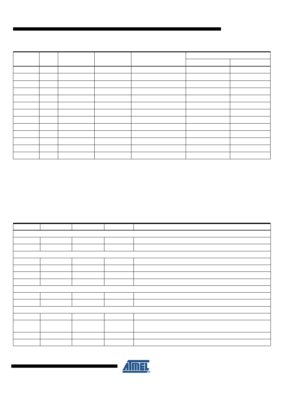
Table 3-2.
Signal Description
Pin Number
Pin Name
Type
Active Level Pin Description/Comment
RF Section
D1
RF
ANALOG IN
-
Input from SAW filter
C1
NRF
ANALOG IN
-
Inverted input from SAW filter
GPS XTAL Section
A1
XTO
ANALOG IN
-
XTO input (23.104 MHz)/optional TCXO input
B3
NXTO
ANALOG IN
-
Inverted XTO input (23.104 MHz)/optional TCXO input
A2
X
ANALOG OUT
-
XTO interface (capacitor)
B2
NX
ANALOG OUT
-
Inverted XTO interface (capacitor)
RTC Section
A12
XT_IN
ANALOG IN
-
Oscillator input (32.768 kHz)
B12
XT_OUT
ANALOG OUT
-
Oscillator output (32.768 kHz)
Automatic Gain Control, bandwidth setting
A4
AGCO
ANALOG IO
-
Automatic gain control analog voltage, connect shunt capacitor to GND
D4 EGC
DIGITAL
IN
-
Enable external gain control
(high = software gain control, low = automatic gain control)
G12
AGCOUT0
DIGITAL OUT
-
Software gain control
C4
SDI
DIGITAL IN
-
Software gain control
Table 3-1.
ATR0630P1 Pinout (Continued)
Pin Name
BGA 96
Pin Type
Pull Resistor
(Reset Value)
(1)
Firmware Label
PIO Bank A
I
O
Notes:
1. PD = internal pull-down resistor, PU = internal pull-up resistor, OH = switched to Output High at reset
2. VBAT18 represent the internal power supply of the backup power domain.
3. VDD_USB is the supply voltage for following the USB pins: USB_DM and USB_DP. For operation of the USB interface, sup-
ply of 3.0V to 3.6V is required.
4. VDDIO is the supply voltage for the following GPIO pins: P1, P2, P8, P12, P14, P16, P17, P18, P19, P20, P21, P23, P24,
P25, P26, P27 and P29.