Detailed description, Pin description – Rainbow Electronics MAX5821 User Manual
Page 7
Detailed Description
The MAX5822 is a dual, 12-bit, voltage-output DAC with
an I
2
C/SMBus-compatible 2-wire interface. The device
consists of a serial interface, power-down circuitry, two
input and DAC registers, two 12-bit resistor string
DACs, two unity-gain output buffers, and output resistor
networks. The serial interface decodes the address and
control bits, routing the data to the proper input or DAC
register. Data can be directly written to the DAC regis-
ter, immediately updating the device output, or can be
written to the input register without changing the DAC
output. Both registers retain data as long as the device
is powered.
DAC Operation
The MAX5822 uses a segmented resistor string DAC
architecture, which saves power in the overall system
and guarantees output monotonicity. The MAX5822’s
input coding is straight binary, with the output voltage
given by the following equation:
where N = 12 (bits), and D = the decimal value of the
input code (0 to 4095).
Output Buffer
The MAX5822 analog outputs are buffered by preci-
sion, unity-gain followers that slew 0.5V/µs. Each buffer
output swings rail-to-rail, and is capable of driving 5k
Ω
in parallel with 200pF. The output settles to ±0.5LSB
within 4µs.
Power-On Reset
The MAX5822 features an internal POR circuit that ini-
tializes the device upon power-up. The DAC registers
are set to zero scale and the device is powered down,
with the output buffers disabled and the outputs pulled
to GND through the 100k
Ω termination resistor.
Following power-up, a wake-up command must be initi-
ated before any conversions are performed.
Power-Down Modes
The MAX5822 has three software-controlled, low-power
power-down modes. All three modes disable the output
buffers and disconnect the DAC resistor strings from
REF, reducing supply current draw to 1µA and the ref-
erence current draw to less than 1µA. In power-down
mode 0, the device output is high impedance. In
power-down mode 1, the device output is internally
pulled to GND by a 1k
Ω termination resistor. In power-
down mode 2, the device output is internally pulled to
GND by a 100k
Ω termination resistor. Table 1 shows
the power-down mode command words.
Upon wake-up, the DAC output is restored to its previ-
ous value. Data is retained in the input and DAC regis-
ters during power-down mode.
Digital Interface
The MAX5822 features an I
2
C/SMBus-compatible 2-
wire interface consisting of a serial data line (SDA) and
a serial clock line (SCL). The MAX5822 is SMBus com-
patible within the range of V
DD
= 2.7V to 3.6V. SDA and
SCL facilitate bidirectional communication between the
MAX5822 and the master at rates up to 400kHz. Figure
1 shows the 2-wire interface timing diagram. The
MAX5822 is a transmit/receive slave-only device, rely-
ing upon a master to generate a clock signal. The mas-
ter (typically a microcontroller) initiates data transfer on
the bus and generates SCL to permit that transfer.
A master device communicates to the MAX5822 by
transmitting the proper address followed by command
and/or data words. Each transmit sequence is framed
by a START (S) or repeated START (S
r
) condition and a
STOP (P) condition. Each word transmitted over the
V
V
D
OUT
REF
N
_
( )
=
×
2
MAX5822
Dual, 12-Bit, Low-Power, 2-Wire, Serial
Voltage-Output DAC
_______________________________________________________________________________________
7
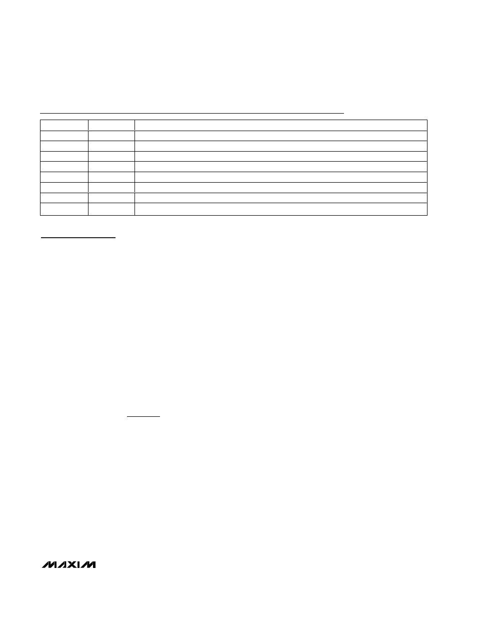
PIN
NAME
FUNCTION
1
V
DD
Power Supply
2
GND
Ground
3
ADD
Address Select. A logic high sets the address LSB to 1; a logic low sets the address LSB to 0
4
SCL
Serial Clock Input
5
SDA
Bidirectional Serial Data Interface
6
REF
Reference Input
7
OUTA
DAC A Output
8
OUTB
DAC B Output
Pin Description