Rainbow Electronics MAX5085 User Manual
Page 2
MAX5084/MAX5085
65V, 200mA, Low-Quiescent-Current
Linear Regulators in TDFN
2
_______________________________________________________________________________________
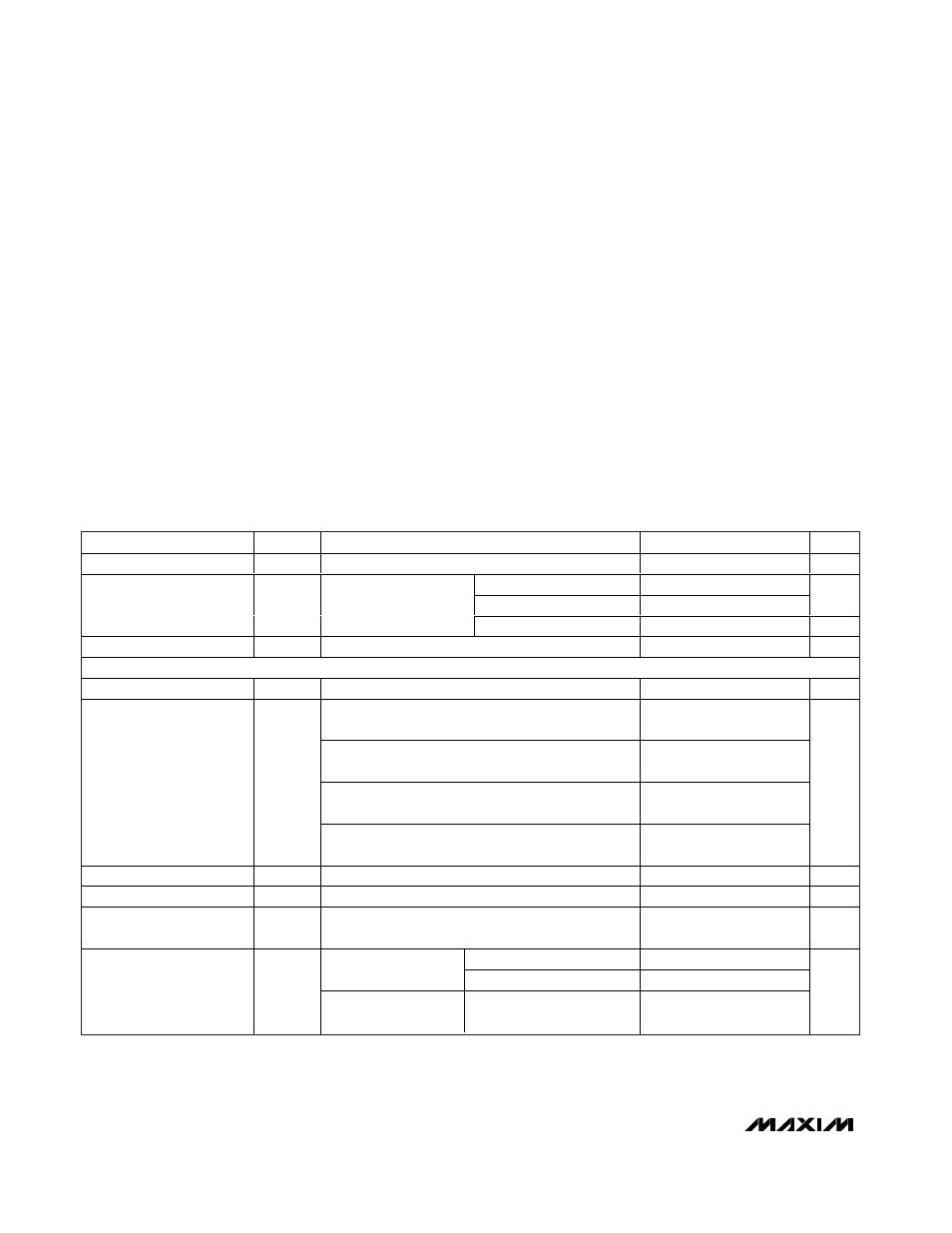
ABSOLUTE MAXIMUM RATINGS
ELECTRICAL CHARACTERISTICS
(V
IN
= 14V, I
OUT
= 1mA, C
IN
= C
OUT
= 10µF, V
EN
= 2.4V, T
A
= T
J
= -40°C to +125°C, unless otherwise noted. Typical specifications
are at T
A
= +25°C, unless otherwise noted.) (Note 1)
Stresses beyond those listed under “Absolute Maximum Ratings” may cause permanent damage to the device. These are stress ratings only, and functional
operation of the device at these or any other conditions beyond those indicated in the operational sections of the specifications is not implied. Exposure to
absolute maximum rating conditions for extended periods may affect device reliability.
IN to GND ...............................................................-0.3V to +80V
EN to GND..............................................................-0.3V to +80V
SET, OUT, OUT_SENSE
to GND................-0.3V to the lesser of (V
IN
+ 0.3V) or +13.2V
OUT_SENSE to OUT..............................................-0.3V to +0.3V
Short-Circuit Duration (V
IN
≤ 65V)..............................Continuous
Maximum Current into Any Pin (except IN and OUT).......±20mA
Continuous Power Dissipation (T
A
= +70°C)
6-Pin TDFN-EP (derate 23.8mW/°C above +70°C) ...1904.8mW*
Thermal Resistance:
θ
JA
................................................................................42°C/W
θ
JC
...............................................................................8.5°C/W
Operating Temperature Range .........................-40°C to +125°C
Junction Temperature ......................................................+150°C
Storage Temperature Range .............................-65°C to +150°C
Lead Temperature (soldering, 10s) .................................+300°C
PARAMETER
SYMBOL
CONDITIONS
MIN
TYP
MAX
UNITS
Input Voltage Range
V
IN
V
IN
> V
OUT
+ 1.5V
6.5
65
V
I
OUT
= 0
51
140
I
OUT
= 100µA
51
140
µA
Supply Current
I
Q
Measured at GND,
SET = GND
I
OUT
= 200mA
2
4
mA
Shutdown Supply Current
I
SHDN
V
EN
≤ 0.4V
6
16
µA
REGULATOR
Guaranteed Output Current
I
OUT
V
OUT
= V
OUT(NOM)
±4%
200
mA
V
IN
= 9V to 16V, SET = GND, I
OUT
= 5mA to 200mA,
OUT_SENSE connected to OUT (MAX5084)
4.8
5.0
5.2
V
I N
= 6.5V to 21V , S E T = GN D , I
OU T
= 5m A to 100m A,
OUT_SENSE connected to OUT (MAX5084)
4.85
5.0
5.15
V
IN
= 9V to 16V, SET = GND, I
OUT
= 5mA to 50mA,
OUT_SENSE connected to OUT (MAX5084)
4.9
5.1
Output Voltage Accuracy
V
OUT
V
IN
= 6.5V, SET = GND, I
OUT
= 1mA to 200mA,
OUT_SENSE connected to OUT (MAX5085)
3.168
3.300
3.432
V
Output Voltage Range
I
OUT
= 5mA, adjustable output
2.54
11
V
Dropout Voltage
∆V
DO
I
OUT
= 200mA, V
OUT
= 5V, MAX5084 (Note 2)
0.9
1.5
V
Startup Response Time
Rising edge of V
IN
to rising edge of V
OUT
,
R
L
= 500
Ω (Note 3)
400
µs
MAX5084, SET = GND
-1
+1
V
IN
from 8V to 65V
MAX5085, SET = GND
-0.5
+0.5
Line Regulation
∆V
OUT
/
∆V
IN
V
IN
from 14V to 65V
Adjustable output from
2.54V to 11V
-0.5
+0.5
mV/V
*As per JEDEC51 Standard (Multilayer Board).