Block diagram – Rainbow Electronics T89C51IC2 User Manual
Page 2
2
T89C51IC2
Rev. C – 3-Dec-01
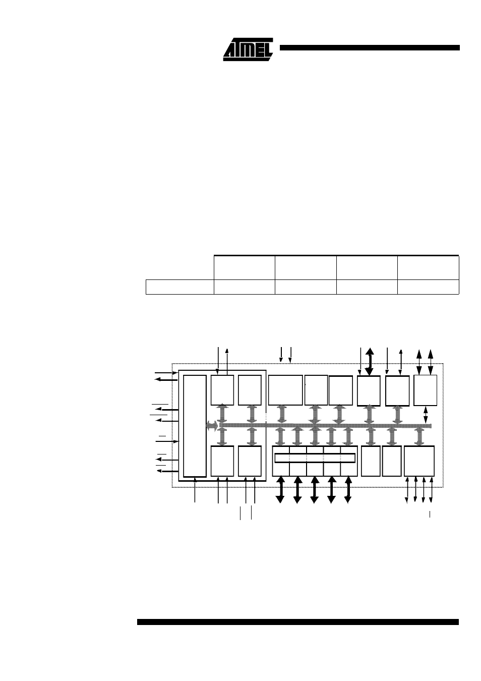
In addition, the T89C51IC2 has a 32kHz Subsidiary clock Oscillator, a Programmable
Counter Array, an XRAM of 1024 byte, a Hardware Watchdog Timer, a Keyboard Inter-
face, a I2C Interface, a SPI Interface, a more versatile serial channel that facilitates
multiprocessor communication (EUART) and a speed improvement mechanism (X2
mode).
The fully static design of the T89C51IC2 allows to reduce system power consumption by
bringing the clock frequency down to any value, even DC, without loss of data.
The T89C51IC2 has 2 software-selectable modes of reduced activity and 8 bit clock
prescaler for further reduction in power consumption. In the Idle mode the CPU is frozen
while the peripherals and the interrupt system are still operating. In the power-down
mode the RAM is saved and all other functions are inoperative.
The added features of the T89C51IC2 make it more powerful for applications that need
pulse width modulation, high speed I/O and counting capabilities such as alarms, motor
control, corded phones, smart card readers.
Table 1. Memory Size
Block Diagram
PLCC44
VQFP44 1.4
Flash (bytes)
XRAM (bytes)
TOTAL RAM
(bytes)
I/O
T89C51IC2
32k
1024
1280
34
Timer 0
INT
RAM
256x8
T0
T1
Rx
D
Tx
D
WR
RD
EA
PSEN
ALE/
XTAL2
XTAL1
EUART
CPU
Timer 1
IN
T
1
Ctrl
IN
T
0
( 2)
( 2)
C51
CORE
(2) (2)
(2) ( 2)
Port 0
P0
Port 1 Port 2 Port 3
Parallel I/O Ports & Ext. Bus
P1
P2
P3
XRAM
1Kx8
IB-bus
PCA
RE
S
E
T
PROG
Watch
Dog
PC
A
EC
I
Vs
s
V
CC
(2)
(2)
( 1)
(1): Alternate function of Port 1
(2): Alternate function of Port 3
(1)
Timer2
T2
E
X
T2
(1)
(1)
Port I2
PI
2
F las h
32K x8 or
16K x8
Key
B oard
ROM
2Kx8
Boot
+
BRG
SPI
MI
S
O
MO
S
I
SC
K
(1) (1) (1)
SS
( 1)
I
2
C
SD
A
SC
L