Pin description, Typical operating characteristics (continued) – Rainbow Electronics MAX4981 User Manual
Page 6
MAX4978–MAX4981
Overvoltage Protector with
Active Current Limit
6
_______________________________________________________________________________________
Pin Description
PIN
MAX4978/
MAX4979
MAX4980/
MAX4981
NAME
FUNCTION
1
1
IN
Supply Voltage Input. IN powers the charge pump required to turn on the internal FET.
When the correct adapter is plugged in, a 160ms debounce timer prevents a false turn-on of
the internal FET. Bypass IN to GND with a 1µF ceramic capacitor as close to the device as
possible to enable ±15kV (HBM) ESD protection.
2
—
SDT
Startup Debounce Time Indicator.
SDT is an active-low open-drain output that asserts low
during the debounce/autoretry time.
—
2
BAT
Battery Monitor Input. Connect BAT to Li-ion battery terminal. Bypass BAT to GND with a 1µF
ceramic capacitor as close to the device as possible to enable ±15kV (HBM) ESD protection.
3, 6, 7
3, 6, 7
I.C.
Internally Connected. Connect I.C. to GND.
4
4
EN
Acti ve- Low E nab l e Inp ut. D r i ve
E N l ow for nor m al op er ati on. D r i ve E N hi g h to d i sab l e the d evi ce.
5
5
GND
Ground
8
8
OUT
Output Voltage. Output of internal FET.
—
—
EP
Exposed Pad. Internally connected to GND. Connect EP to a large ground plane to maximize
thermal performance. Do not use EP as the sole GND connection.
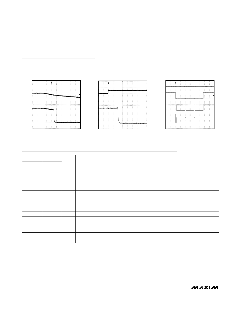
Typical Operating Characteristics (continued)
(V
IN
= 5.0V,
EN = GND, T
A
= +25°C, unless otherwise noted.)
UNDERVOLTAGE FAULT RESPONSE
MAX4978-81 toc10
4
μs/div
2V/div
2V/div
V
IN
V
OUT
BATTERY OVERVOLTAGE FAULT RESPONSE
MAX4978-81 toc11
2
μs/div
R
L
= 1k
Ω
2V/div
2V/div
V
BAT
V
OUT
SHORT-CIRCUIT RESPONSE
MAX4978-81toc12
100ms/div
5V/div
5V/div
1A/div
V
IN
V
OUT
I
OUT
V
SDT