Rainbow Electronics MAX4981 User Manual
Page 2
MAX4978–MAX4981
Overvoltage Protector with
Active Current Limit
2
_______________________________________________________________________________________
ABSOLUTE MAXIMUM RATINGS
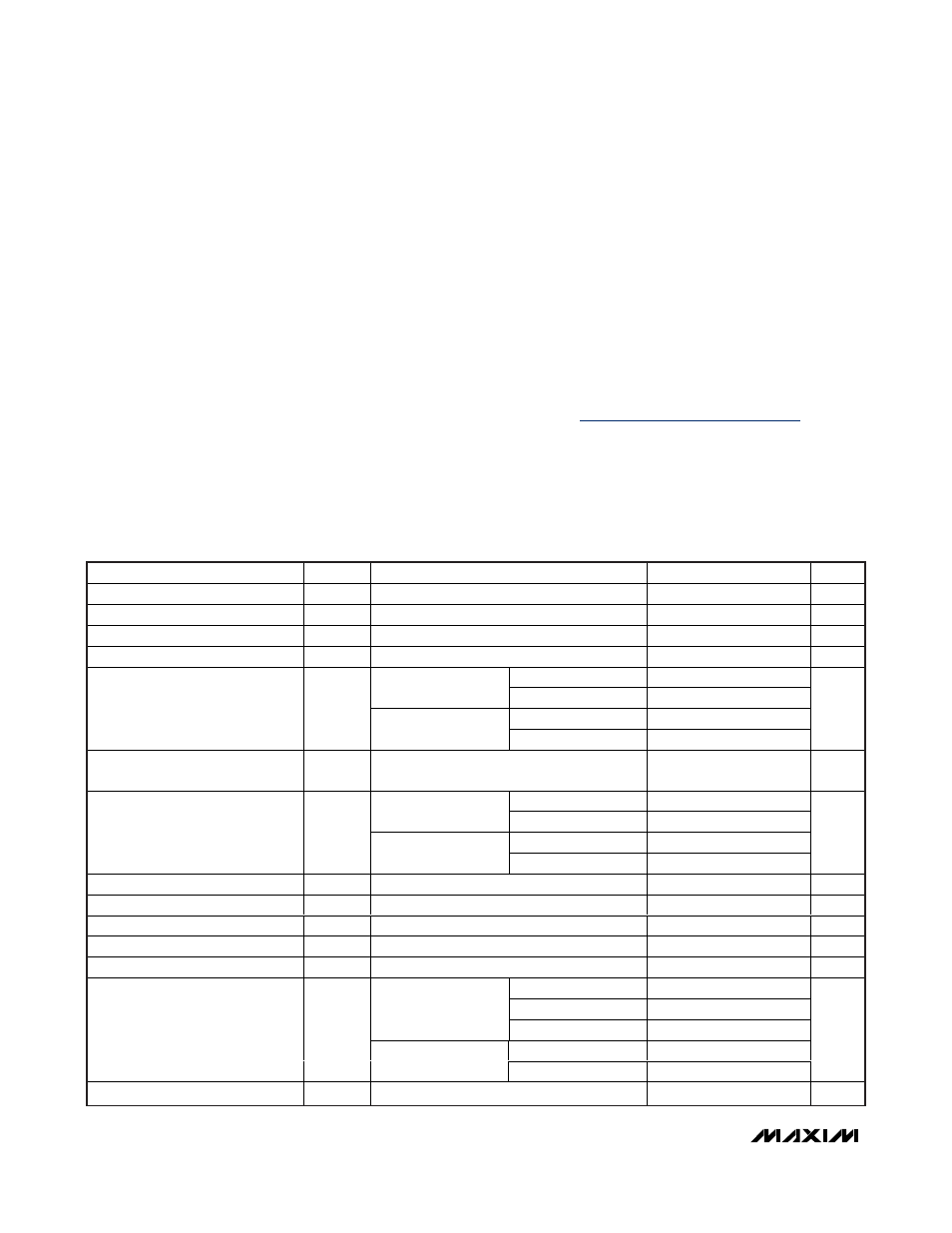
ELECTRICAL CHARACTERISTICS
(V
IN
= 5.0V, V
EN
= 0V, T
A
= -40°C to +85°C, unless otherwise noted. Typical values are at T
A
= +25°C.) (Note 2)
Stresses beyond those listed under “Absolute Maximum Ratings” may cause permanent damage to the device. These are stress ratings only, and functional
operation of the device at these or any other conditions beyond those indicated in the operational sections of the specifications is not implied. Exposure to
absolute maximum rating conditions for extended periods may affect device reliability.
(Voltages referenced to GND.)
IN,
SDT ................................................................. -0.3V to +30V
OUT ........................................................................... -0.3V to IN
EN, BAT .................................................................. -0.3V to +6V
SDT Continuous Current ................................................. ±50mA
Continuous Power Dissipation (T
A
= +70°C)
8-Pin 2mm x 3mm TDFN (derate 16.7mW/°C
above +70°C) ........................................................... 1333mW
Junction-to-Case Thermal Resistance (
θ
JC
) (Note 1)
8-Pin 2mm x 3mm TDFN ......................................... 10.8°C/W
Junction-to-Ambient Thermal Resistance (
θ
JA
) (Note 1)
8-Pin 2mm x 3mm TDFN ............................................ 60°C/W
Operating Temperature Range ......................... -40°C to +85°C
Junction Temperature .................................................... +150°C
Storage Temperature Range ........................... -65°C to +150°C
Lead Temperature (soldering, 10s) ................................+300°C
PARAMETER
SYMBOL
CONDITIONS
MIN
TYP
MAX
UNITS
Input Voltage Range
V
IN
2.3
28
V
Input Supply Current
I
IN
I
OUT
< I
LIM_MIN
130
190
µA
UVLO Supply Current
I
UVLO
V
IN
= 2.3V
35
60
µA
Shutdown Supply Current
I
SHDN
V
EN
= 5V
15
23
µA
V
IN
falling
4.2
MAX4978
V
IN
rising
4.3
4.4
4.5
V
IN
falling
2.5
IN Undervoltage Lockout
V
UVLO
MAX4979/MAX4980/
MAX4981
V
IN
rising
2.56
2.63
2.70
V
IN Undervoltage Lockout
Hysteresis
1
%
V
IN
falling
5.5
MAX4978/MAX4980/
MAX4981
V
IN
rising
5.6
5.7
5.8
V
IN
falling
6.5
IN Overvoltage Lockout
V
OVLO
MAX4979
V
IN
rising
6.65
6.80
6.95
V
IN Overvoltage Lockout Hysteresis
1
%
BAT Overvoltage Trip Level
V
BOTL
MAX4980/MAX4981, V
BAT
rising
4.3
4.4
4.5
V
BAT Overvoltage Hysteresis
MAX4980/MAX4981
1
%
BAT Input Leakage Current
I
LKGB
MAX4980/MAX4981, V
BAT
= 4.2V
1
µA
Switch On-Resistance
R
ON
I
OUT
= 100mA
85
160
m
Ω
T
A
=+25°C
850
900
950
T
A
= 0°C to +85°C
800
1000
MAX4978, MAX4979,
MAX4980
T
A
= -40°C to +0°C
780
1000
T
A
=+25°C
1850
1950
2050
Overcurrent Protection Threshold
I
LIM
MAX4981
T
A
= -40°C to +85°C
1750
1950
2150
mA
Thermal Shutdown
T
SHDN
T
A
rising
160
°C
Note 1: Package thermal resistances were obtained using the method described in JEDEC specification JESD51-7, using a 4-layer
board. For detailed information on package thermal considerations, refer to
www.maxim-ic.com/thermal-tutorial
.