Absolute maximum ratings, Electrical characteristics – Rainbow Electronics MAX4885E User Manual
Page 2
MAX4885E
Ultra-Low Capacitance 1:2 VGA
Switch with ±15kV ESD
2
_______________________________________________________________________________________
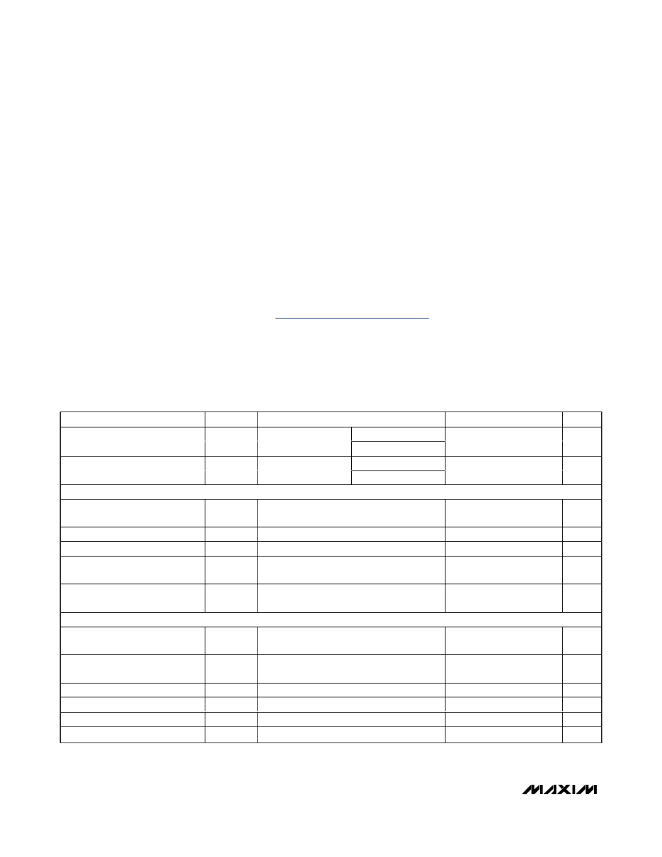
ABSOLUTE MAXIMUM RATINGS
Stresses beyond those listed under “Absolute Maximum Ratings” may cause permanent damage to the device. These are stress ratings only, and functional
operation of the device at these or any other conditions beyond those indicated in the operational sections of the specifications is not implied. Exposure to
absolute maximum rating conditions for extended periods may affect device reliability.
(All voltages referenced to GND.)
V
CC
, V
L
.....................................................................-0.3V to +6V
R_, G_, B_, SDA1, SCL1, SDA2, SCL2,
H1, V1, (Note 1) ........................................-0.3V to V
CC
+ 0.3V
H0, V0, SDA0, SCL0, EN, SEL.........................-0.3V to V
L
+ 0.3V
Continuous Current through RGB Switches .....................±30mA
Continuous Current through DDC Switches .....................±30mA
Peak Current through RGB Switches
(pulsed at 1ms, 10% duty cycle)...................................±90mA
Peak Current through DDC Switches (pulsed at 1ms,
10% duty cycle)............................................................±90mA
Continuous Power Dissipation (T
A
= +70°C)
24-Pin TQFN (derate 27.8mW/°C above +70°C) ........2222mW
Junction to Ambient Thermal Resistance (
θ
JA
) (Note 2)
24-Pin TQFN..................................................................36°C/W
Junction to Ambient Thermal Resistance (
θ
JC
) (Note 2)
24-Pin TQFN....................................................................3°C/W
Operating Temperature Range ...........................-40°C to +85°C
Storage Temperature Range .............................-65°C to +150°C
Junction Temperature ......................................................+150°C
Lead Temperature (soldering, 10s) .................................+300°C
ELECTRICAL CHARACTERISTICS
(V
CC
= +5.0V ±10%, V
L
= +2V to +5.5V, T
A
= T
MIN
to T
MAX
, unless otherwise noted. Typical values are at V
CC
= +5.0V, V
L
= +3.3V and
T
A
= +25°C.) (Note 3)
PARAMETER
SYMBOL
CONDITIONS
MIN
TYP
MAX
UNITS
EN = V
L
V
CC
Quiescent Supply Current
I
CC
V
CC
= +5.0V
EN = GND
1
µA
EN = V
L
V
L
Quiescent Supply Current
I
VL
V
L
= +3.3V
EN = GND
1
µA
RGB ANALOG SWITCHES
On-Resistance
R
ON
V
CC
= +5.0V, I
IN
= -10mA, V
IN
= +0.7V
(Note 4)
6
Ω
On-Resistance Matching
ΔR
ON
0
≤ V
IN
≤ 0.7V, I
IN
= -10mA
0.5
Ω
On-Resistance Flatness
R
FLAT(ON)
0
≤ V
IN
≤ 0.7V, I
IN
= -10mA
0.5
Ω
Off-Leakage Current
I
L(OFF)
V
CC
= +5.5V, V
IN
= +0.3V or +5.5V,
V
EN
= 0 or V
L
-1
+1
µA
On-Leakage Current
I
L(ON)
V
CC
= +5.5V, V
IN
= +0.3V or +5.5V,
V
EN
= V
L
-1
+1
µA
HV BUFFER
Input Voltage Low
V
ILHV
0.33 x
V
L
V
Input Voltage High
V
IHHV
0.66 x
V
L
V
Input Logic Hysteresis
V
HYST
75
mV
Input Leakage Current
I
INHV
V
CC
= +5.5V, V
L
= +5.5V, V
IN
= 0 or V
L
-1
+1
µA
High-Output Drive Current
I
OHHV
V
OHHV
≥ 3.0V
8.0
mA
Low-Output Drive Current
I
OLHV
V
OLHV
≤ 0.6V
8.0
mA
Note 1: Signals exceeding V
CC
or GND are clamped by internal diodes. Limit forward-diode current to maximum current rating.
Note 2: Package thermal resistances were obtained using the method described in JEDEC specifications. For detailed information
on package thermal considerations, refer to
www.maxim-ic.com/thermal-tutorial
.