Table 1. input shift register – Rainbow Electronics MAX5223 User Manual
Page 8
MAX5223
Low-Power, Dual, 8-Bit, Voltage Output
Serial DAC in 8-Pin SOT23
8
_______________________________________________________________________________________
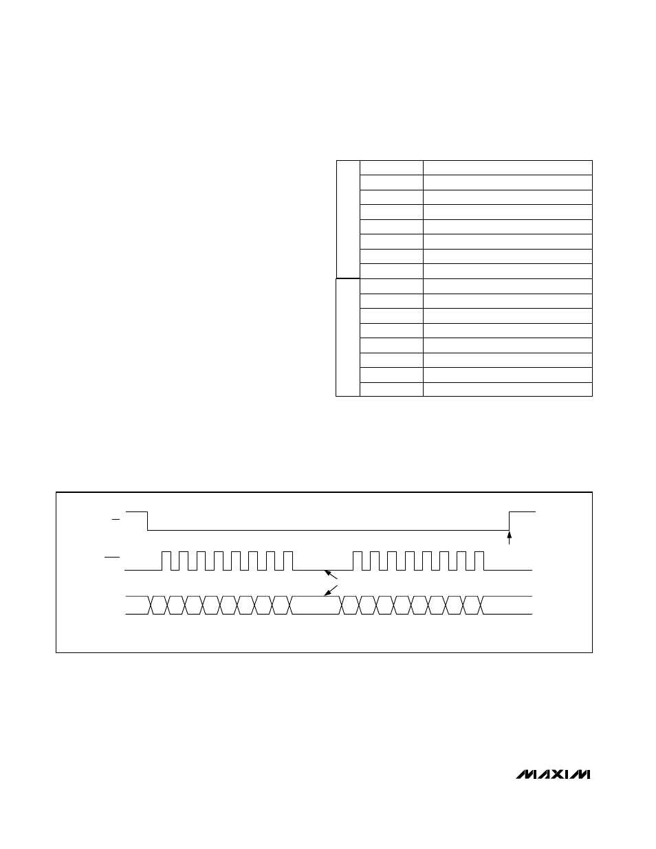
in starting with UB1 (uncommitted bit), followed by the
remaining control bits and the data byte. The least sig-
nificant bit (LSB) of the data byte (D0) is the last bit
clocked into the shift register (Figure 2).
Table 3 is an example of a 16-bit input word. It per-
forms the following functions:
• 80 hex (128 decimal) loaded into DAC registers
A and B.
• DAC A and DAC B are active.
Table 4 shows code examples and how to calculate
their corresponding outputs.
*Clocked in last
**Clocked in first
Uncommitted Bit 1
UB1**
Uncommitted Bit 2
UB2
Uncommitted Bit 3
UB3
Shutdown, Active-High
SB
Shutdown, Active-High
SA
Uncommitted Bit 4
UB4
Load Reg DAC B, Active-High
LB
Load Reg DAC A, Active-High
LA
DAC Data Bit 7 (MSB)
D7
DAC Data Bit 6
D6
DAC Data Bit 5
D5
DAC Data Bit 4
D4
DAC Data Bit 3
D3
DAC Data Bit 2
D2
DAC Data Bit 1
D1
DAC Data Bit 0 (LSB)
D0*
Table 1. Input Shift Register
DIN
SCLK
CS
UB1 UB2 UB3
SB
SA
UB4
LB
LA
D7
D6
D5
D4
D3
D2
D1
D0
OPTIONAL
(CONTROL BYTE)
(DATA BYTE)
INSTRUCTION
EXECUTED
Figure 2. 3-Wire Serial-Interface Timing Diagram
DATA BITS
CONTROL BITS