Typical operating characteristics (continued), Pin description – Rainbow Electronics MAX5223 User Manual
Page 6
MAX5223
Low-Power, Dual, 8-Bit, Voltage Output
Serial DAC in 8-Pin SOT23
6
_______________________________________________________________________________________
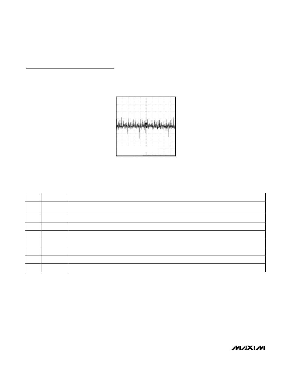
Typical Operating Characteristics (continued)
(V
DD
= +3V, T
A
= +25°C, unless otherwise noted.)
2ms/div
OUTPUT VOLTAGE NOISE (DC TO 1MHz)
MAX5223 toc16
CH1
OUTA
2mV/div
AC-COUPLED
V
DD
= +3V, REF = V
DD
, NO LOAD,
DIGITAL CODE = FF
______________________________________________________________Pin Description
DAC A Output Voltage (Buffered)
OUTA
5
DAC B Output Voltage (Buffered)
OUTB
6
Reference Input for DAC A and DAC B (Optional: Bypass with 0.1µF to GND)
REF
7
Serial Data Input of the 16-Bit Shift Register. Data is clocked into the register on the rising edge of SCLK.
DIN
8
Serial Clock Input
SCLK
4
Positive Power Supply (+2.7V to +5.5V). Bypass with 0.22µF to GND.
V
DD
3
PIN
Ground
GND
2
Chip Select. Active-Low. Enables data to be shifted into the 16-bit shift register. Programming commands
are executed at the rising edge of
–
C
—
S
–
.
–
C
—
S
–
1
FUNCTION
NAME