Rainbow Electronics MAX6632 User Manual
Page 6

MAX6629–MAX6632
12-Bit + Sign Digital Temperature Sensors
with Serial Interface
6
_______________________________________________________________________________________
finish.
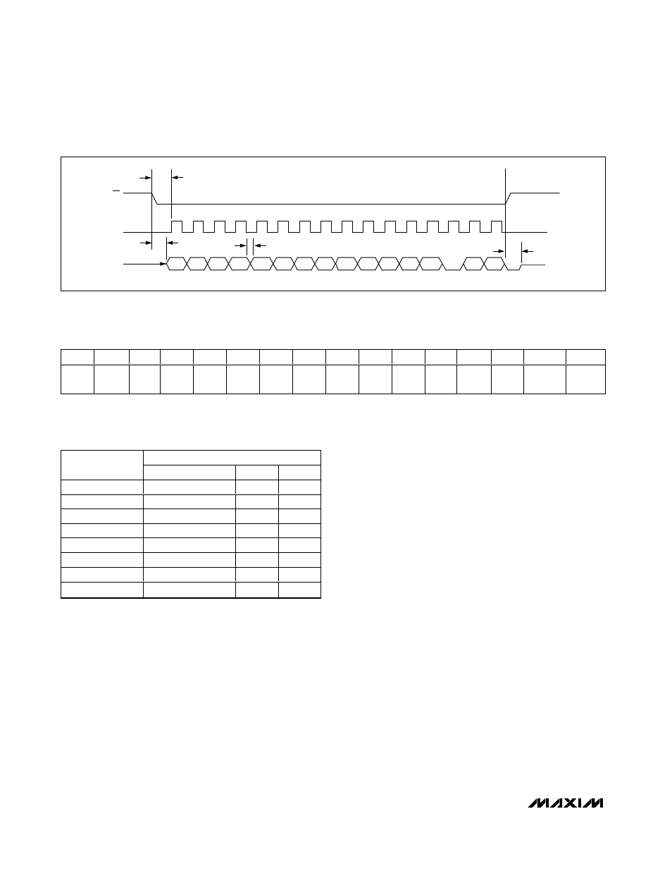
CS’s falling edge stops any conversion in
progress, and data is latched into the shift register.
Then the data clocks out at SO on SCK’s falling edge
with the sign bit (D15) first, followed by the MSB. Data
is sent in one 16-bit word, and
CS must remain low until
all 16 bits are transferred. If
CS goes high in the middle
of a transmission, it is necessary to wait the conversion
time (less than 300ms) before attempting a new read.
The serial data is composed of 12 + 1 data bits
(D15–D3) and 3 trailing bits (D2–D0). D2 is always low,
serving as the confirmation bit that the device has been
communicated with. The last 2 bits, D0 and D1, are
undefined and are always in high-impedance mode
(Table 1). The power-up state for SO is high imped-
ance. Figure 3 shows the detailed serial timing specifi-
cations for the SPI port. The temperature data format is
in two's complement format (Table 2).
Power Shutdown Mode
The MAX6629–MAX6632 do not have a built-in power
software shutdown mode. However, a power shutdown
mode is easily implemented utilizing an unused logic
gate. A typical CMOS or TTL logic output has enough
drive capability to serve as the power source if its out-
put voltage level exceeds 3V, as shown in Figure 1.
Drive the logic output low to provide a hardware shut-
down mode.
Idle Mode
The MAX6629–MAX6632 can be put into idle mode by
pulling
CS low. Data can be clocked out when the
device is in idle mode.
Power-On Reset (POR)
The POR supply voltage of the MAX6629–MAX6632 is
typically 1.6V. Below this supply voltage the interface is
inactive and the data register is set to the POR state,
0°C.
When power is first applied and V
CC
rises above 1.6V
(typ), the device starts to convert, although temperature
reading is not recommended at V
CC
levels below 3.0V.
Figure 3. SPI Timing Diagram
D15
D0
D1
D2
D3
SCK
SO
t
DV
t
CSS
t
DO
CS
t
TR
D15
D14
D13
D12
D11
D10
D9
D8
D7
D6
D5
D4
D3
D2
D1
D0
Sign
MSB
Data
LSB
Data
Low
High-Z
High-Z
Table 1. Data Output Format
Table 2. Temperature Data Format
(Two’s Complement)
DIGITAL OUTPUT (BINARY)
TEMPERATURE
(°C)
D15–D3
D2
D1, D0
150
0,1001,0110,0000
0
XX
125
0,0111,1101,0000
0
XX
25
0,0001,1001,0000
0
XX
0.0625
0,0000,0000,0001
0
XX
0
0,0000,0000,0000
0
XX
-0.0625
1,1111,1111,1111
0
XX
-25
1,1110,0111,0000
0
XX
-55
1,1100,1001,0000
0
XX
