Electrical characteristics, Absolute maximum ratings – Rainbow Electronics MAX7360 User Manual
Page 2
I
2
C-Interfaced Key-Switch Controller and LED
Driver/GPIOs with Integrated ESD Protection
MAX7360
2 ______________________________________________________________________________________
Stresses beyond those listed under “Absolute Maximum Ratings” may cause permanent damage to the device. These are stress ratings only, and functional operation of the device at these
or any other conditions beyond those indicated in the operational sections of the specifications is not implied. Exposure to absolute maximum rating conditions for extended periods may
affect device reliability.
V
CC
to GND ............................................................. -0.3V to +4V
COL0–COL7, ROW0–ROW7 to GND ...................... -0.3V to +4V
SDA, SCL, AD0, INTI, INTK to GND ........................ -0.3V to +6V
PORT0–PORT7 to GND ......................................... -0.3V to +16V
All Other Pins to GND ................................-0.3V to (V
CC
+ 0.3V)
DC Current on PORT0–PORT7, COL2–COL7 ....................25mA
GND Current .......................................................................80mA
Continuous Power Dissipation (T
A
= +70NC)
40-Pin TQFN (derate 22.2mW/NC above +70NC).......1777mW
36-Bump WLP (derate 21.7mW/NC above +70NC) ....1739mW
Junction-to-Case Thermal Resistance (B
JC
) (Note 1)
40-Pin TQFN ..................................................................2NC/W
36-Bump WLP ................................................................... N/A
Junction-to-Ambient Thermal Resistance (B
JA
) (Note 1)
40-Pin TQFN ................................................................45NC/W
36-Bump WLP .............................................................46NC/W
Operating Temperature Range .......................... -40NC to +85NC
Junction Temperature .....................................................+150NC
Storage Temperature Range ............................ -65NC to +150NC
ESD Protection
Human Body Model (R
D
= 1.5kI, C
S
= 100pF)
All Pins .............................................................................Q2kV
IEC61000-4-2 (R
D
= 330I, C
S
= 150pF)
Contact Discharge
ROW0–ROW7, COL0–COL7, PORT0–PORT7 to GND ....Q8kV
Air-Gap Discharge
ROW0–ROW7, COL0–COL7, PORT0–PORT7 to GND ..Q15kV
Lead Temperature (soldering, 10s)
40-Pin TQFN ................................................................+300NC
36-Bump WLP ........................................................... (Note 2)
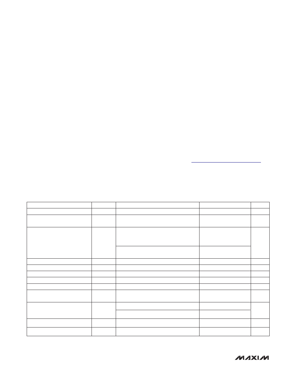
ELECTRICAL CHARACTERISTICS
(V
CC
= +1.62V to +3.6V, T
A
= -40NC to +85NC, unless otherwise noted. Typical values are at V
CC
= +3.3V, T
A
= +25NC.) (Notes 3, 4)
ABSOLUTE MAXIMUM RATINGS
Note 1: Package thermal resistances were obtained using the method described in JEDEC specification JESD51-7, using a single-
layer board. For detailed information on package thermal considerations, refer to
www.maxim-ic.com/thermal-tutorial
.
Note 2: Refer to Pb-free solder-reflow requirements described in J-STD-020, Rev D.1, or any other paste supplier specification.
PARAMETER
SYMBOL
CONDITIONS
MIN
TYP
MAX
UNITS
Operating Supply Voltage
V
CC
1.62
3.3
3.6
V
External Supply Voltage
PORT0–PORT7
V
PORT_
14
V
Operating Supply Current
I
CC
All key switches open, oscillator running,
COL2–COL7 configured as key switches,
V
PORT
_ = V
CC
34
50
F
A
N keys pressed
34 +
20 x N
Sleep-Mode Supply Current
I
SL
1.3
3
F
A
Key-Switch Source Current
I
KEY
20
35
F
A
Key-Switch Source Voltage
V
KEY
0.43
0.5
V
Key-Switch Resistance
R
KEY
(Note 5)
5
kI
Startup Time from Shutdown
t
START
2
2.4
ms
Output Low Voltage
COL2–COL7
V
OL
I
SINK
= 10mA
0.5
V
Oscillator Frequency (PWM
Clock)
f
OSC
T
A
= +25NC, V
CC
= +2.61V
125
128
131
kHz
T
A
= T
MIN
- T
MAX
, V
CC
P 3.6V
102
164
Oscillator Frequency Variation
D
f
OSC
T
A
= +25NC
-6
+8.5
%
Key-Scan Frequency
f
KEY
Derived from oscillator clock
64
kHz