Table 3. 2-wire interface address map – Rainbow Electronics MAX7360 User Manual
Page 14
I
2
C-Interfaced Key-Switch Controller and LED
Driver/GPIOs with Integrated ESD Protection
MAX7360
14 _____________________________________________________________________________________
is required on SDA. The MAX7360’s SCL line operates
only as an input. A pullup resistor is required on SCL if
there are multiple masters on the 2-wire interface, or if
the master in a single-master system has an open-drain
SCL output.
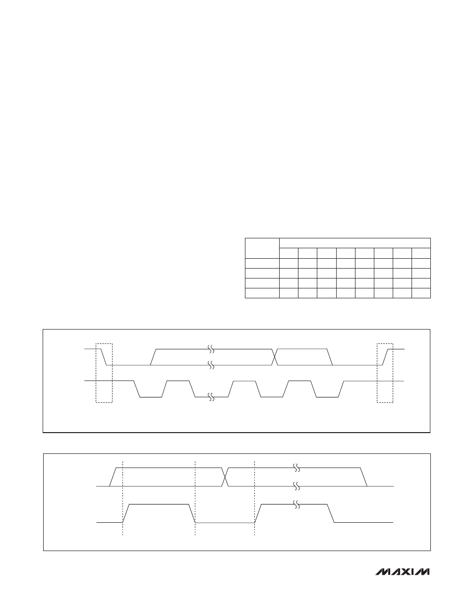
Each transmission consists of a START condition (Figure
3) sent by a master, followed by the MAX7360 7-bit slave
address plus R/W bit, a register address byte, one or
more data bytes, and finally, a STOP condition.
START and STOP Conditions
Both SCL and SDA remain high when the interface is not
busy. A master signals the beginning of a transmission
with a START (S) condition by transitioning SDA from
high to low while SCL is high. When the master has
finished communicating with the slave, it issues a STOP
(P) condition by transitioning SDA from low to high while
SCL is high. The bus is then free for another transmission.
Bit Transfer
One data bit is transferred during each clock pulse
(Figure 4). The data on SDA must remain stable while
SCL is high.
Acknowledge
The acknowledge bit is a clocked 9th bit (Figure 4), which
the recipient uses to handshake receipt of each byte of
data. Thus, each byte transferred effectively requires
9 bits. The master generates the 9th clock pulse, and
the recipient pulls down SDA during the acknowledge
clock pulse; therefore, the SDA line is stable low during
the high period of the clock pulse. When the master is
transmitting to the MAX7360, the MAX7360 generates the
acknowledge bit because the MAX7360 is the recipient.
When the MAX7360 is transmitting to the master, the
master generates the acknowledge bit because the
master is the recipient.
Figure 3. START and STOP Conditions
Figure 4. Bit Transfer
Table 3. 2-Wire Interface Address Map
PIN AD0
DEVICE ADDRESS
A7
A6
A5
A4
A3
A2
A1
A0
GND
0
1
1
1
0
0
0
R/W
V
CC
0
1
1
1
0
1
0
R/W
SDA
0
1
1
1
1
0
0
R/W
SCL
0
1
1
1
1
1
0
R/W
SDA
SCL
START
CONDITION
STOP
CONDITION
S
P
SDA
SCL
DATA LINE STABLE;
DATA VALID
CHANGE OF DATA
ALLOWED