Electrical characteristics (continued) – Rainbow Electronics MAX16030 User Manual
Page 3

MAX16025–MAX16030
Dual-/Triple-/Quad-Voltage, Capacitor-
Adjustable, Sequencing/Supervisory Circuits
_
__
__
__
__
__
__
__
__
__
__
__
__
__
__
__
__
__
__
__
__
__
__
__
__
__
__
__
__
__
__
__
__
__
__
__
__
__
__
__
__
__
__
__
__
__
__
__
__
__
__
__
__
__
__
__
__
__
__
__
__
__
__
__
__
__
__
__
__
__
__
__
__
__
__
__
__
__
__
__
__
__
__
__
__
__
__
_
3
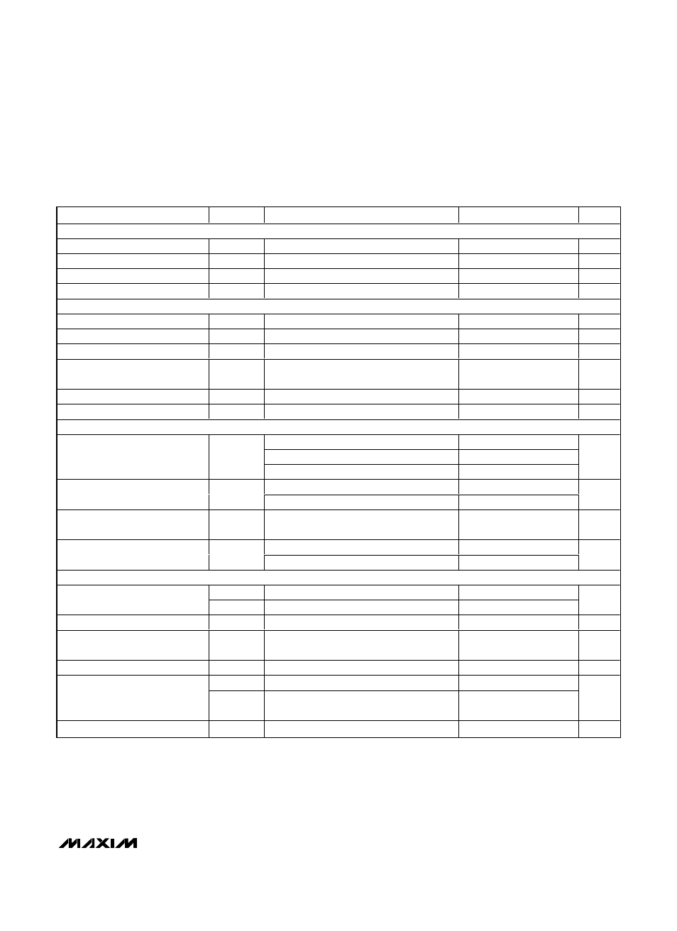
ELECTRICAL CHARACTERISTICS (continued)
(V
CC
= 2.2V to 28V, T
A
= -40°C to +125°C, unless otherwise specified. Typical values are at V
CC
= 3.3V and T
A
= +25°C.) (Note 1)
PARAMETER
SYMBOL
CONDITIONS
MIN
TYP
MAX
UNITS
CRESET AND CDLY_
CRESET Threshold
V
TH-RESET
CRESET rising, V
CC
= 3.3V
0.465
0.5
0.535
V
CRESET Charge Current
I
CH-RESET
V
CC
= 3.3V
380
500
620
nA
CDLY_ Threshold
V
TH-CDLY
CDLY_ rising, V
CC
= 3.3V
0.95
1
1.05
V
CDLY_ Charge Current
I
CH-CDLY
V
CC
= 3.3V
200
250
300
nA
DIGITAL LOGIC INPUTS (EN_,
MR, TOL, TH1, TH0)
Input Low Voltage
V
IL
0.4
V
Input High Voltage
V
IH
1.4
V
TH1, TH0 Logic-Input Floating
0.6
V
TOL, TH1, TH0 Logic-Input
Current
V
TOL
, V
TH1
, V
TH0
= GND or V
CC
-1
+1
µA
EN_ Input Leakage Current
V
EN_
= V
CC
or GND
-100
+100
nA
MR Internal Pullup Current
V
CC
= 3.3V
250
535
820
nA
OUTPUTS (OUT_,
RESET)
V
CC
≥ 1.2V, I
SINK
= 90µA
0.3
V
CC
≥ 2.25V, I
SINK
= 0.5mA
0.3
Output Low Voltage (Open-Drain
or Push-Pull)
V
OL
V
CC
≥ 4.5V, I
SINK
= 1mA
0.35
V
V
CC
≥ 3V, I
SOURCE
= 500µA
0.8 x V
CC
Output High Voltage (Push-Pull)
V
OH
V
CC
≥ 4.5V, I
SOURCE
= 800µA
0.8 x V
CC
V
Output Leakage Current (Open-
Drain)
I
LKG
Output not asserted low, V
OUT
= 28V
1
µA
CRESET = V
CC
, V
CC
= 3.3V
140
190
260
Reset Timeout Period
t
RP
CRESET open
0.030
ms
TIMING
t
DELAY+
IN_ rising, CDLY_ open
35
IN_ to OUT_ Propagation Delay
t
DELAY-
IN_ falling, CDLY_ open
20
µs
IN_ to RESET Propagation Delay
t
RST-DELAY
CRESET open, IN_ falling
35
µs
MR Minimum Input Pulse Width
(Note 3)
2
µs
EN_ or MR Glitch Rejection
280
ns
t
OFF
From device enabled to device disabled
3
EN_ to OUT_ Delay
t
ON
From device disabled to device enabled
(CDLY_ open)
30
µs
MR to RESET Delay
MR falling
3
µs
Note 1: Devices are production tested at T
A
= +25°C. Limits over temperature are guaranteed by design.
Note 2: Operating below the UVLO causes all outputs to go low. The outputs are guaranteed to be in the correct state for V
CC
down
to 1.2V.
Note 3: In order to guarantee an assertion, the minimum input pulse width must be greater than 2µs.
