Rainbow Electronics MAX19506 User Manual
Page 22

MAX19506
Dual-Channel, 8-Bit, 100Msps ADC
22
______________________________________________________________________________________
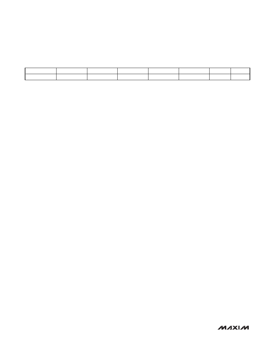
Clock Divide/Data Format/Test Pattern (06h)
Reserved (07h)—Do not write to this register
BIT 7
BIT 6
BIT 5
BIT 4
BIT 3
BIT 2
BIT 1
BIT 0
TEST_PATTERN
TEST_DATA
FORMAT_1
FORMAT_0
TERM_100
SYNC_MODE
DIV1
DIV0
Bit 7
TEST_PATTERN: Test pattern selection
0 = Ramps from 0 to 255 (offset binary) and repeats (subsequent formatting applied) (default)
1 = Data alternates between D[7:0] = 01010101, DOR = 1, and D[7:0] = 10101010,
DOR = 0 on both channels
Bit 6
TEST_DATA: Data test mode
0 = Normal data output (default)
1 = Outputs test data pattern
Bit 5, 4
FORMAT_1, FORMAT_0: Data numerical format
00 = Two’s complement (default)
01 = Offset binary
10 = Gray code
11 = Two’s complement
Bit 3
TERM_100: Select 100
Ω clock input termination
0 = No termination (default)
1 = 100
Ω termination across differential clock inputs
Bit 2
SYNC_MODE: Divider synchronization mode select
0 = Slip mode (Figure 11) (default)
1 = Edge mode (Figure 12)
Bit 1, 0
DIV1, DIV0: Input clock-divider select
00 = No divider (default)
01 = Divide-by-2
10 = Divide-by-4
11 = No divider
