Microprocessor-compatible, 14-bit dacs, Detailed description, Applications information – Rainbow Electronics MX7535 User Manual
Page 6
MX7534/MX7535
_______________Detailed Description
Digital-to-Analog Section
The basic MX7534/MX7535 digital-to-analog converter
(DAC) circuit consists of a laser-trimmed, thin-film,
11-bit R-2R resistor array, a 3-bit segmented resistor
array, and NMOS current switches, as shown in Figure
2. The three MSBs are decoded to drive switches A–G
of the segmented array, and the remaining bits drive
switches S0–S10 of the R-2R array.
Binary weighted currents are switched to either AGNDF
or I
OUT
, depending on the status of each input bit. The
R-2R ladder current is one-eighth of the total reference
input current. The remaining seven-eighths of the cur-
rent flows in the segmented resistors, dividing equally
among these seven resistors. The input resistance at
REF is constant; therefore, it can be driven by a voltage
or current source of positive or negative polarity.
The MX7534/MX7535 are optimized for unipolar output
operation (analog output from 0V to -V
REF
), although
bipolar operation (analog output from +V
REF
to -V
REF
) is
possible with some added external components.
Figure 3 shows the equivalent circuit for the two DACs.
C
OUT
varies from about 90pF to 180pF, depending on
the digital code. R
0
denotes the DAC’S equivalent out-
put resistance, which varies with the input code.
g(V
REF,
N) is the Thevenin equivalent voltage generator
due to the reference input voltage, V
REF
, and the trans-
fer function of the R-2R ladder, N.
Digital Section
All digital inputs are both TTL and 5V CMOS logic compat-
ible. The digital inputs are protected from electrostatic dis-
charge (ESD) with typical input currents of less than 1nA.
To minimize power-supply currents, keep digital input volt-
ages as close to 0V and 5V logic levels as possible.
__________Applications Information
Unipolar Operation (2-Quadrant
Multiplication)
Figures 4a and 4b show the circuit diagram for unipolar
binary operation. With an AC input, the circuit performs
2-quadrant multiplication. The code table for Figure 4 is
given in Table 2.
Capacitor C1 provides phase compensation and helps
prevent overshoot and ringing when high-speed op
amps are used. Note that the output polarity is the
inverse of the reference input.
Microprocessor-Compatible,
14-Bit DACs
6
_______________________________________________________________________________________
V
IH
+
V
IL
2
NOTES:
1) ALL INPUT-SIGNAL RISE AND FALL TIMES ARE MEASURED FROM 10% TO 90%
OF +5V. t
R
= t
F
= 20ns.
2) TIMING MEASUREMENT REFERENCE LEVEL IS
t
5
t
6
t
7
t
1
t
2
t
3
t
4
CS
5V
A0,A1
DATA
0V
5V
0V
5V
0V
5V
0V
WR
t
3
t
6
t
5
t
6
t
5
t
4
t
2
t
1
t
1
t
2
t
4
5V
0V
5V
0V
5V
0V
5V
0V
NOTES:
1) ALL INPUT-SIGNAL RISE AND FALL TIMES ARE MEASURED FROM 10% TO 90%
OF +5V. t
R
= t
F
= 20ns.
2) TIMING MEASUREMENT REFERENCE LEVEL IS
3) IF LDAC IS ACTIVATED PRIOR TO THE RISING EDGE OF WR, THEN IT MUST
STAY LOW FOR t
3
OR LONGER AFTER WR GOES HIGH.
V
IH
+
V
IL
2
CSLSB
CSMSB
LDAC
WR
DATA
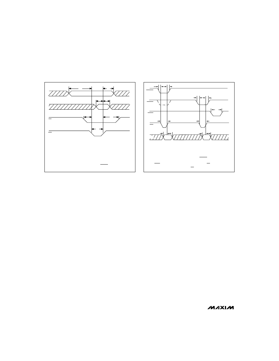
Figure 1a. MX7534 Timing Diagram
Figure 1b. MX7535 Timing Diagram