Electrical characteristics (continued) – Rainbow Electronics MX7535 User Manual
Page 3
MX7534/MX7535
Microprocessor-Compatible,
14-Bit DACs
_______________________________________________________________________________________
3
mV
-200
-500
V
SS
Negative Supply-Voltage Range
V
11.4
15.75
V
DD
Positive Supply-Voltage Range
mA
3
4
I
DD
Positive Supply Current
µA
500
I
SS
Negative Supply Current
UNITS
MIN
TYP
MAX
SYMBOL
PARAMETER
For specific performance
For specific performance
MX7534
MX7535
Digital inputs at 0V or V
DD
CONDITIONS
Digital inputs at
V
INH
or V
INL
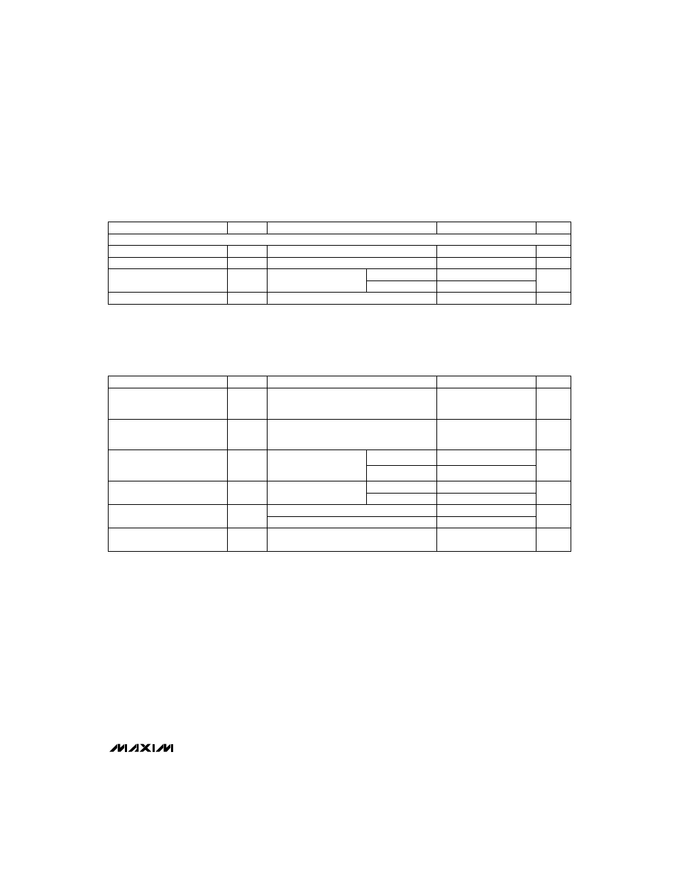
ELECTRICAL CHARACTERISTICS (continued)
(V
DD
= +11.4V to +15.75V (Note 1), V
REF
= 10V, V
IOUT
= V
AGNDS
= V
SS
= 0V, T
A
= T
MIN
to T
MAX
, unless otherwise noted.)
mVp-p
3
nV-sec
50
µs
0.8
1.5
Output Current Setting Time
Digital-to-Analog Glitch Impulse
nV/Hz
15
Output Noise Voltage Density
(10Hz–100kHz)
130
C
OUT
Output Capacitance (IOUT Pin)
5
Multiplying Feedthrough Error
(Note 5)
%/%
±0.01
±0.02
Power-Supply Rejection
pF
260
UNITS
MIN
TYP
MAX
SYMBOL
PARAMETER
T
A
= +25°C
Measured with V
REF
= 0V,
IOUT loads = 100
Ω
II
13pF, DAC register
alternately loaded with all 1s and all 0s
T
A
= +25°C, to 0.003% of full-scale range,
IOUT load = 100
Ω
II
13pF, DAC register
alternately loaded with all 1s and all 0s
Measured between R
FB
and I
OUT
DAC register loaded with all 0s
T
A
= T
MIN
to T
MAX
T
A
= +25°C
T
A
= T
MIN
to T
MAX
DAC register loaded with all 1s
CONDITIONS
V
REF
= ±10V, 10kHz
sine wave, DAC register
loaded with all 0s
∆
V
DD
= ±5%
Note 1:
Specifications are guaranteed for V
DD
of +11.4V to +15.75V. At V
DD
= +5V, device is still functional with degraded specifications.
Note 2:
Guaranteed by design, not tested.
Note 3:
Resistors have a typical -300ppm/°C tempco.
AC PERFORMANCE CHARACTERISTICS
(Note 4)
(V
DD
= +11.4V to +15.75V, V
REF
= 10V, V
IOUT
= V
AGND
(V
AGNDS
for MX7535) = V
SS
= 0V, output amplifier is AD544*,
T
A
= T
MIN
to T
MAX
, unless otherwise noted.)
Note 4:
These characteristics are included for design guidance only, and are not subject to test.
Note 5:
Feedthrough can be further reduced by connecting the metal lid on the ceramic package to DGND.
* AD544 is an Analog Devices part.
POWER REQUIREMENTS