Pin description – Rainbow Electronics MAX15020 User Manual
Page 8

MAX15020
2A, 40V Step-Down DC-DC Converter with
Dynamic Output-Voltage Programming
8
_______________________________________________________________________________________
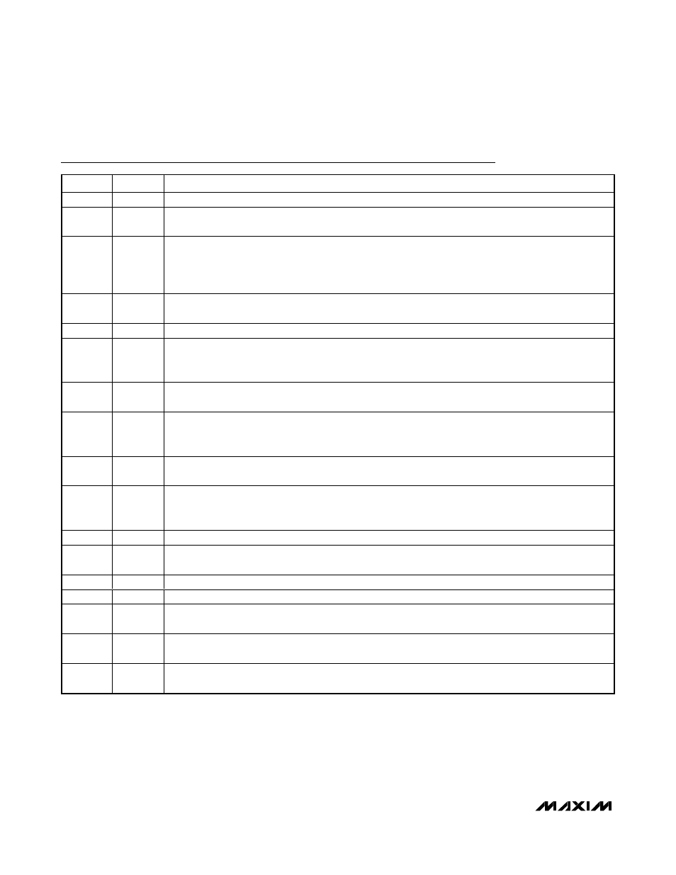
Pin Description
PIN
NAME
FUNCTION
1
COMP
Voltage-Error-Amplifier Output. Connect COMP to the necessary compensation feedback network.
2
FB
Feedback Regulation Point. Connect to the center tap of an external resistor-divider connected between
the output and GND to set the output voltage. The FB voltage regulates to the voltage applied to REFIN.
3
ON/OFF
ON/OFF Control. The ON/OFF rising threshold is set to approximately 1.225V. Connect to the center tap of
a resistive divider connected between IN and GND to set the turn-on (rising) threshold. Connect ON/OFF to
GND to shut down the IC. Connect ON/OFF to IN for always-on operation given that V
IN
has risen above the
UVLO threshold. ON/OFF can be used for power-supply sequencing.
4
REFOUT
0.98V Reference Voltage Output. Bypass REFOUT to GND with a 0.1µF ceramic capacitor. REFOUT is to
be used only with REFIN. It is not to be used to power any other external circuitry.
5
SS
Soft-Start. Connect a 0.01µF or greater ceramic capacitor from SS to GND. See the Soft-Start (SS) section.
6
REFIN
External Reference Input. Connect to an external reference. V
FB
regulates to the voltage applied to REFIN.
Connect REFIN to REFOUT to use the internal 1V reference. See the Reference Input and Output (REFIN,
REOUT) section.
7
FSEL
Internal Switching Frequency Selection Input. Connect FSEL to REG to select f
SW
= 300kHz. Connect FSEL
to GND to select f
SW
= 500kHz. When an external clock is connected to SYNC connect FSEL to REG.
8
SYNC
Oscillator Synchronization Input. SYNC can be driven by an external 100kHz to 500kHz clock to
synchronize the MAX15020’s switching frequency. Connect SYNC to GND to disable the synchronization
function. When using SYNC, connect FSEL to REG.
9
DVREG
Power Supply for Internal Digital Circuitry. Connect a 10Ω resistor from REG to DVREG. Connect DVREG to
the anode of the boost diode, D2 in Figure 2. Bypass DVREG to GND with at least a 1µF ceramic capacitor.
10
PGND
Power-Ground Connection. Connect the input filter capacitor’s negative terminal, the anode of the
freewheeling diode, and the output filter capacitor’s return to PGND. Connect externally to GND at a single
point near the input bypass capacitor’s return terminal.
11
N.C.
No Connection. Leave unconnected or connect to GND
12
BST
High-Side Gate Driver Supply. Connect BST to the cathode of the boost diode and to the positive terminal
of the boost capacitor.
13, 14, 15
LX
Source Connection of Internal High-Side Switch. Connect the inductor and rectifier diode’s cathode to LX.
16, 17, 18
IN
Supply Input Connection. Connect to an external voltage source from 7.5V to 40V.
19
REG
8V Internal Regulator Output. Bypass to GND with at least a 1µF ceramic capacitor. Do not use REG to
power external circuitry.
20
GND
Ground Connection. Solder the exposed pad to a large GND plane. Connect GND and PGND together at
one point near the input bypass capacitor return terminal.
—
EP
Exposed Pad. Connect EP to GND. Connecting EP does not remove the requirement for proper ground
connections to the appropriate pins. See the PCB Layout and Routing section.
