Detailed description, Pin description – Rainbow Electronics MAX5083 User Manual
Page 7
MAX5082/MAX5083
1.5A, 40V, MAXPower Step-Down
DC-DC Converters
_______________________________________________________________________________________
7
Detailed Description
The MAX5082/MAX5083 are voltage-mode buck con-
verters with internal 0.3
Ω power MOSFET switches. The
MAX5082 has a wide input voltage range of 4.5V to
40V. The MAX5083’s input voltage range is 7.5V to 40V.
The internal low R
DS_ON
switch allows for up to 1.5A of
output current. The 250kHz fixed switching frequency,
external compensation, and voltage feed-forward sim-
plify loop compensation design and allow for a variety
of L and C filter components. Both devices offer an
automatic switchover to pulse-skipping (PFM) mode,
providing low quiescent current and high efficiency at
light loads. Under no load, a PFM mode operation
reduces the current consumption to only 1.4mA. In
shutdown, the supply current falls to 200µA. Additional
features include an externally programmable undervolt-
age lockout through the ON/OFF pin, a programmable
soft-start, cycle-by-cycle current limit, hiccup mode
output short-circuit protection, and thermal shutdown.
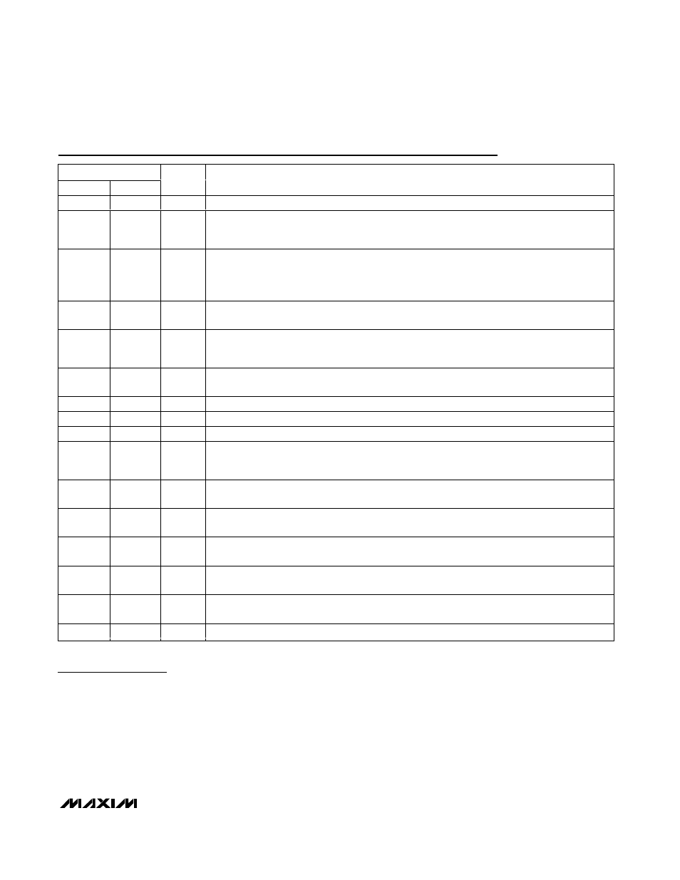
PIN
MAX5082
MAX5083
NAME
FUNCTION
1
1
COMP
Error Amplifier Output. Connect COMP to the compensation feedback network.
2
2
FB
Feedback Regulation Point. Connect to the center tap of a resistive divider from converter
output to SGND to set the output voltage. The FB voltage regulates to the voltage present at SS
(1.23V).
3
3
ON/OFF
ON/OFF and External UVLO Control. The ON/OFF rising threshold is set to approximately 1.23V.
Connect to the center tap of a resistive divider from IN to SGND to set the UVLO (rising)
threshold. Pull ON/OFF to SGND to shut down the device. ON/OFF can be used for power-
supply sequencing. Connect to IN for always-on operation.
4
4
SS
Soft-Start and Reference Output. Connect a capacitor from SS to SGND to set the soft-start
time. See the Applications Information section to calculate the value of the SS capacitor.
5
5
SYNC
Oscillator Synchronization Input. SYNC can be driven by an external 150kHz to 350kHz clock to
synchronize the MAX5082/MAX5083’s switching frequency. Connect SYNC to SGND when not
used.
6
6
DVREG
Gate Drive Supply for High-Side MOSFET Driver. Connect externally to REG for MAX5082.
Connect to REG and the anode of the boost diode for MAX5083.
7
—
C+
Charge-Pump Flying Capacitor Positive Connection
8
—
C-
Charge-Pump Flying Capacitor Negative Connection
—
7, 8
N.C.
No Connection. Not internally connected. Can be left floating or connected to SGND.
9
9
PGND
Power Ground Connection. Connect the input filter capacitor’s negative terminal, the anode of
the freewheeling diode, and the output filter capacitor’s return to PGND. Connect externally to
SGND at a single point near the input capacitor’s return terminal.
10
10
BST
High-Side Gate Driver Supply. Connect BST to the cathode of the boost diode and to the
positive terminal of the boost capacitor.
11, 12
11, 12
LX
Source Connection of Internal High-Side Switch. Connect the inductor and rectifier diode’s
anode to LX.
13, 14
13, 14
IN
Supply Input Connection. Connect to an external voltage source from 4.5V to 40V (MAX5082) or
a 7.5V to 40V (MAX5083).
15
15
REG
Internal Regulator Output. 5V output for the MAX5082 and 8V output for the MAX5083. Bypass
to SGND with at least a 1µF ceramic capacitor.
16
16
SGND
Signal Ground Connection. Solder the exposed pad to a large SGND plane. Connect SGND
and PGND together at one point near the input bypass capacitor return terminal.
EP
EP
—
Exposed Pad. Connect exposed pad to SGND.
Pin Description