Absolute maximum ratings, Electrical characteristics – Rainbow Electronics MAX5083 User Manual
Page 2
MAX5082/MAX5083
1.5A, 40V, MAXPower Step-Down
DC-DC Converters
2
_______________________________________________________________________________________
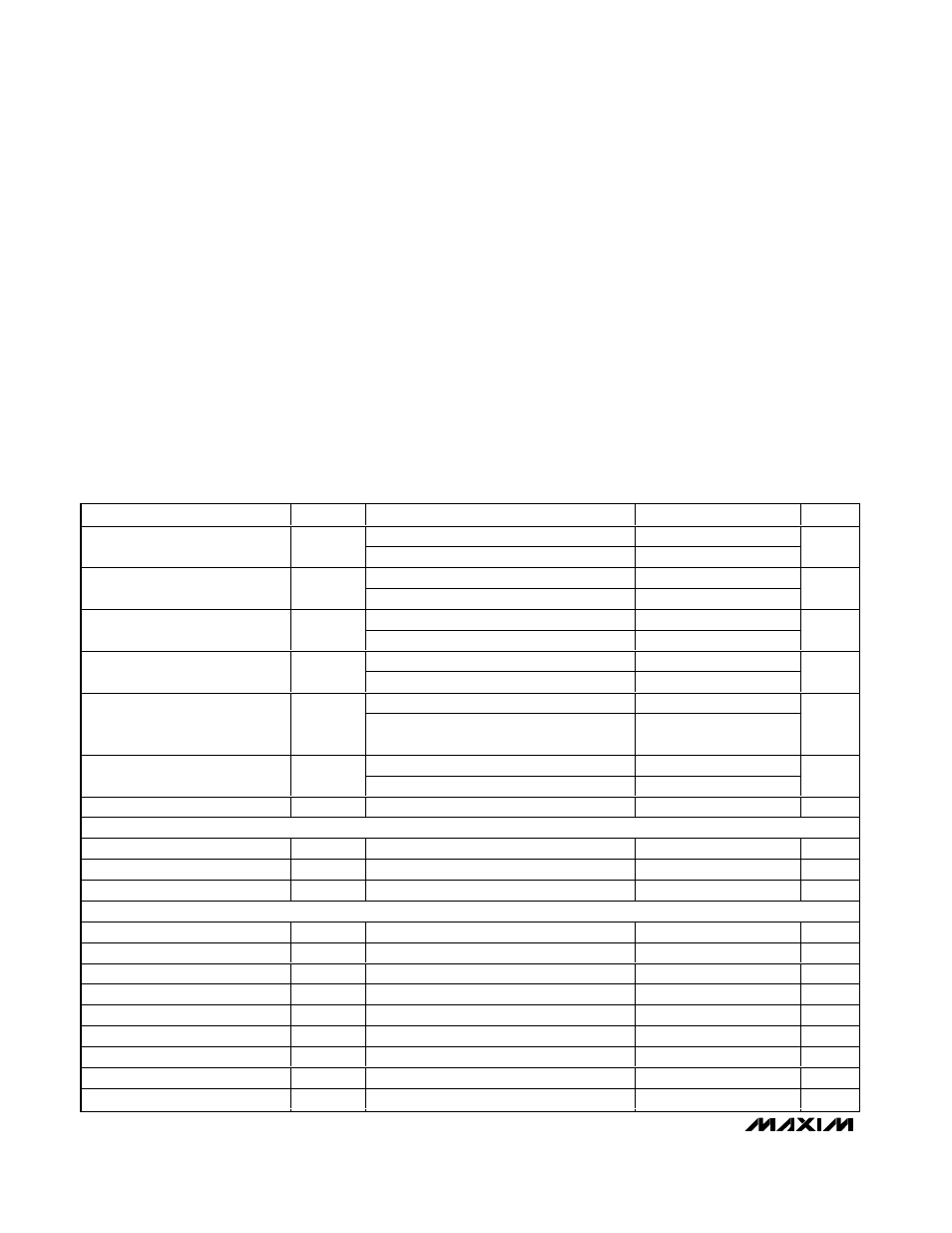
ABSOLUTE MAXIMUM RATINGS
Stresses beyond those listed under “Absolute Maximum Ratings” may cause permanent damage to the device. These are stress ratings only, and functional
operation of the device at these or any other conditions beyond those indicated in the operational sections of the specifications is not implied. Exposure to
absolute maximum rating conditions for extended periods may affect device reliability.
IN, ON/OFF to SGND..............................................-0.3V to +45V
LX to SGND .................................................-0.3V to (V
IN
+ 0.3V)
BST to SGND ................................................-0.3V to (V
IN
+ 12V)
BST to LX................................................................-0.3V to +12V
PGND to SGND .....................................................-0.3V to +0.3V
REG, DVREG, SYNC to SGND ...............................-0.3V to +12V
FB, COMP, SS to SGND ...........................-0.3V to (V
REG
+ 0.3V)
C+ to PGND (MAX5082 only)................(V
DVREG
- 0.3V) to +12V
C- to PGND (MAX5082 only) ................-0.3V to (V
DVREG
+ 0.3V)
Continuous current through internal power MOSFET (pins 11/12
connected together and pins 13/14 connected together)
T
J
= +125°C.........................................................................3A
T
J
= +150°C.........................................................................2A
Continuous Power Dissipation
*
(T
A
= +70°C)
16-Pin TQFN (derate 33.3mW/°C above +70°C) ...2666.7mW
16-Pin TQFN (
θ
JA
)........................................................30°C/W
16-Pin TQFN (
θ
JC
).......................................................1.7°C/W
Operating Temperature Range .........................-40
o
C to +125°C
Maximum Junction Temperature .....................................+150°C
Storage Temperature Range .............................-60°C to +150°C
Lead Temperature (soldering, 10s) .................................+300°C
ELECTRICAL CHARACTERISTICS
(V
IN
= V
ON/OFF
= 12V, V
REG
= V
DVREG
, V
SYNC
= PGND = SGND, T
A
= T
J
= -40°C to +125°C, unless otherwise noted. Typical values
are at T
A
= + 25°C.) (Note 1)
PARAMETER
SYMBOL
CONDITIONS
MIN
TYP
MAX
UNITS
MAX5082
4.5
40
Input Voltage Range
V
IN
MAX5083
7.5
40
V
V
IN
rising, MAX5082
3.9
4.2
Undervoltage Lockout Threshold
UVLO
V
IN
rising, MAX5083
6.8
7.3
V
MAX5082
0.4
Undervoltage Lockout Hysteresis
UVLO
HYST
MAX5083
0.7
V
V
FB
= 0V, MAX5082
10.5
Switching Supply Current (PWM
Operation)
I
SW
V
FB
= 0V, MAX5083
9.5
mA
V
IN
= 12V, V
OUT
= 3.3V, I
OUT
= 1.5A
84
Efficiency
V
IN
= 4.5V, V
OUT
= 3.3V, I
OUT
= 1.5A
(MAX5082)
88
%
MAX5082
1.4
2.5
No-Load Supply Current
(PFM Operation)
MAX5083
1.3
2.3
mA
Shutdown Current
I
SHDN
V
ON/OFF
= 0V, V
IN
= 40V
200
300
µA
ON/
OFF CONTROL
Input Voltage Threshold
V
ON/OFF
V
ON/OFF
rising
1.20
1.23
1.25
V
Input Voltage Hysteresis
0.12
V
Input Bias Current
V
ON/OFF
= 0 to 40V
-250
+250
nA
ERROR AMPLIFIER/SOFT-START
Soft-Start Current
I
SS
8
15
24
µA
Reference Voltage (Soft-Start)
V
SS
1.215
1.228
1.240
V
FB Regulation Voltage
V
FB
I
COMP
= -500µA to +500µA
1.215
1.228
1.240
V
FB Input Range
0
1.5
V
FB Input Current
-250
+250
nA
COMP Voltage Range
I
COMP
= -500µA to +500µA
0.25
4.50
V
Open-Loop Gain
80
dB
Unity-Gain Bandwidth
1.8
MHz
FB Offset Voltage
I
COMP
= -500µA to +500µA
-5
+5
mV
*As per JEDEC 51 Standard.