Detailed description – Rainbow Electronics MAX4885AE User Manual
Page 9
High-Bandwidth, VGA 2:1 Switch
with ±15kV ESD Protection
MAX4885AE
9
Detailed Description
The MAX4885AE integrates high-bandwidth analog
switches and level-translating buffers to implement a
complete 2:1 multiplexer for VGA signals. The device
provides switching for RGB, HSYNC, VSYNC, SDA, and
SCL signals. These signals are required in notebook
VGA switching applications.
The HSYNC and VSYNC inputs feature level-shifting
buffers to support
5V-TTL output logic levels from low-
voltage graphics controllers. These buffered switches
can be driven from +2.0V up to +5.5V. RGB signals are
routed with high-performance analog switches. SDA_
and SCL_ are I
2
C signals with pullups to their respective
voltages. The MAX4885AE protects the low-voltage side
while effectively translating up to the high-voltage level.
Two select inputs are provided to individually select
groups of switches.
RGB, HSYNC, and VSYNC signals are controlled by
SEL1; and both SDA_ and SCL_ signals are controlled
by SEL2.
RGB Switches
The MAX4885AE provides three SPDT high-bandwidth
switches to route standard VGA R_, G_, and B_ signals
(see Table 1). The R_, G_, and B_ analog switches are
identical and any of the three switches can be used to
route red, green, or blue video signals. The R0, G0, and
B0 outputs are ESD protected to Q15kV (HBM).
Horizontal/Vertical Sync Level Shifter
H1, H2, V1, and V2 inputs are buffered to provide level-
shifting and drive capability for horizontal/vertical sync
signals that meet the VESA specification. The H_ and V_
level-shifters are identical, and each level-shifter can be
used for either horizontal or vertical signals. The H0 and
V0 outputs are ESD protected to Q15kV (HBM).
Display-Data Channel Multiplexer
The MAX4885AE provides two logic-level translating
switches to route DDC signals (see Table 2). V
L
is nor-
mally set to +3.3V to provide logic-shifting for VESA
I
2
C-compatible signals. The MAX4885AE protects the
low-voltage graphics controller from +5V that could be
present in VESA-compatible monitors. In some appli-
cations, such as KVM, where logic-level shifting is not
required, then V
L
can
be connected to V
CC
. The SDA_
and SCL_ switches are identical, and each switch can
be used to route either SDA_ or SCL_ signals. The SDA0
and SCL0 outputs are ESD protected to Q15kV (HBM).
ESD Protection
As with all Maxim devices, ESD-protection structures are
incorporated on all pins to protect against electrostatic
discharges encountered during handling and assembly.
Additionally, the R0, G0, B0, H0, V0, SDA0, and SCL0
terminals of the MAX4885AE are designed for protection
to the following limit:
±15kV using the HBM.
For optimum ESD performance, bypass V
CC
and V
L
pins
to ground with 1FF or larger ceramic capacitors as close
as possible to these supply pins.
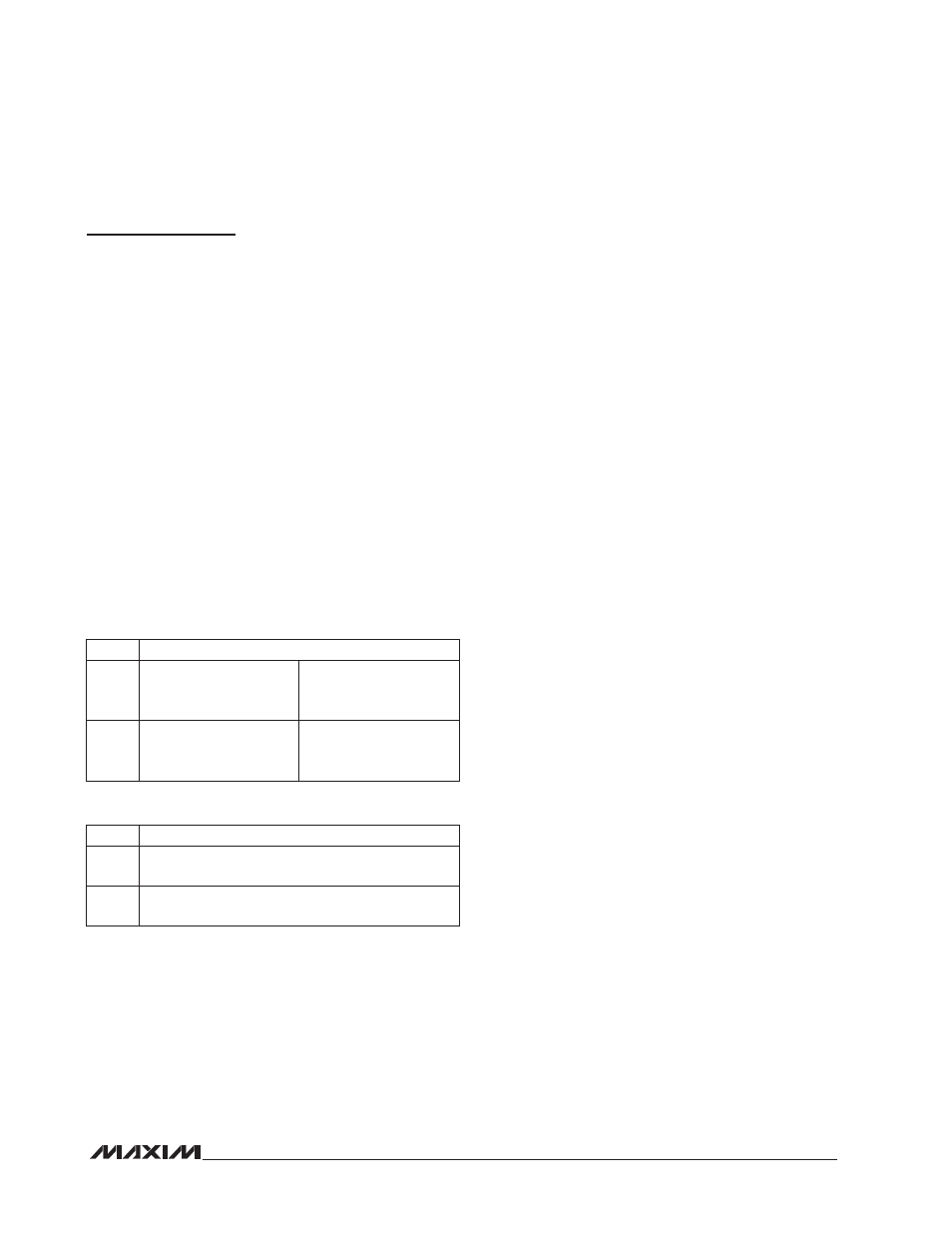
Table 1. RGB/HV Truth Table
Table 2. DDC Truth Table
SEL1
FUNCTION
0
R1 to R0
G1 to G0
B1 to B0
H1 to H0
V1 to V0
1
R2 to R0
G2 to G0
B2 to B0
H2 to H0
V2 to V0
SEL2
FUNCTION
0
SDA1 to SDA0
SCL1 to SCL0
1
SDA2 to SDA0
SCL2 to SCL0