Applications information, Chip information, Package information – Rainbow Electronics MAX4885AE User Manual
Page 10

High-Bandwidth, VGA 2:1 Switch
with ±15kV ESD Protection
MAX4885AE
Maxim cannot assume responsibility for use of any circuitry other than circuitry entirely embodied in a Maxim product. No circuit patent licenses are implied.
Maxim reserves the right to change the circuitry and specifications without notice at any time.
10
Maxim Integrated Products, 120 San Gabriel Drive, Sunnyvale, CA 94086 408-737-7600
©
2009 Maxim Integrated Products
Maxim is a registered trademark of Maxim Integrated Products, Inc.
Human Body Model
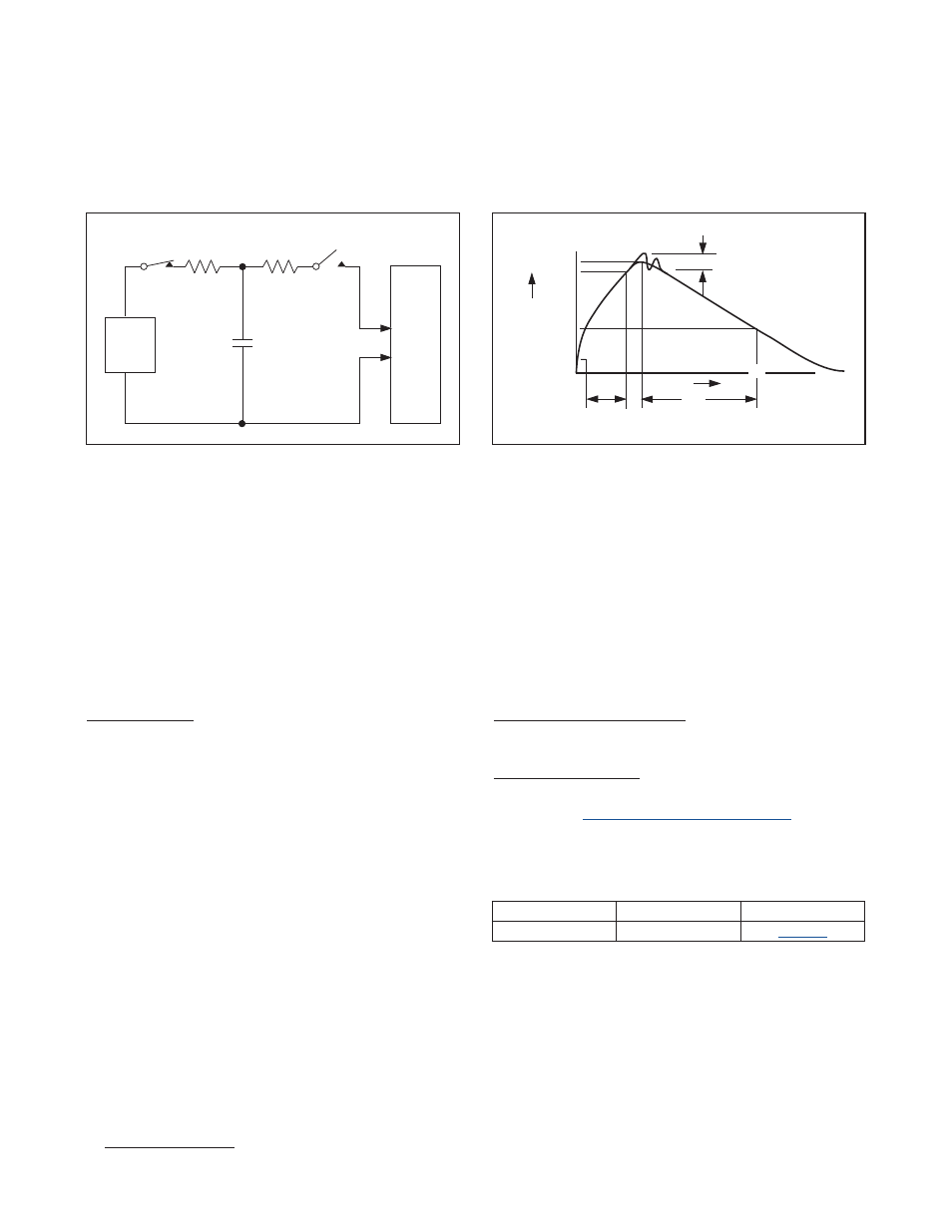
Figure 4 shows the HBM, and Figure 5 shows the cur-
rent waveform it generates when discharged into a low-
impedance state. This model consists of a 100pF capac-
itor charged to the ESD voltage of interest, which is then
discharged into the device through a 1.5kI resistor.
ESD Test Conditions
ESD performance depends on a variety of conditions.
Contact Maxim for a reliability report, test setup, meth-
odology, and results.
Applications Information
The MAX4885AE provides the switching and level-
shifting necessary to drive a standard VGA port from
either an internal graphics controller or an add-in module
(MXM or GPU—see Typical Applications Circuit). The
R_, G_, and B_ signals are switched through the three
low-capacitance SPDT switches. Internal buffers drive
the HSYNC and VSYNC signals to VGA standard 5V-TTL
levels. The DDC multiplexer provides level-shifting.
Connect V
L
to +3.3V for normal operation, or to V
CC
to
disable level-shifting for DDC signals as for KVM appli-
cation.
Power-Supply Decoupling
Bypass each V
CC
pin and V
L
pin to ground with a 1FF
or larger ceramic capacitor as close as possible to the
device.
PCB Layout
High-speed switches such as the MAX4885AE requires
proper PCB layout for optimum performance. Ensure that
impedance-controlled PCB traces for high-speed signals
are matched in length and as short as possible. Connect
the exposed pad to ground or leave unconnected.
Chip Information
PROCESS: BiCMOS
Package Information
For the latest package outline information and land pat-
terns, go to
Note that
a “+”, “#”, or “-” in the package code indicates RoHS
status only. Package drawings may show a different suf-
fix character, but the drawing pertains to the package
regardless of RoHS status.
Figure 4. Human Body ESD Test Model
Figure 5. Human Body Model Current Waveform
CHARGE-CURRENT-
LIMIT RESISTOR
DISCHARGE
RESISTANCE
STORAGE
CAPACITOR
C
S
100pF
R
C
1MΩ
R
D
1.5kΩ
HIGH-
VOLTAGE
DC
SOURCE
DEVICE
UNDER
TEST
I
P
100%
90%
36.8%
t
RL
TIME
t
DL
CURRENT WAVEFORM
PEAK-TO-PEAK RINGING
(NOT DRAWN TO SCALE)
I
r
10%
0
0
AMPERES
PACKAGE TYPE
PACKAGE CODE
DOCUMENT NO.
28 TQFN-EP
T2844+1
