Max5548, Detailed description, Serial interface – Rainbow Electronics MAX5548 User Manual
Page 8: Pin description
MAX5548
Detailed Description
Architecture
The MAX5548 8-bit, dual current-steering DAC (see the
Functional Diagram) operates with DAC update rates
up to 10Msps in SPI mode and 400ksps in I
2
C mode.
The converter consists of a 16-bit shift register and
input DAC registers, followed by a current-steering
array. The current-steering array generates full-scale
currents up to 30mA per DAC. An integrated +1.25V
bandgap reference, control amplifier, and an external
resistor determine each data converter’s full-scale
output range.
Reference Architecture and Operation
The MAX5548 provides an internal +1.25V bandgap ref-
erence or accepts an external reference voltage source
between +0.5V and +1.5V. REFIN serves as the input for
an external low-impedance reference source. Leave
REFIN unconnected in internal reference mode. Internal
or external reference mode is software selectable
through the SPI/I
2
C serial interface.
The MAX5548’s reference circuit (
Figure 1) employs a
control amplifier to regulate the full-scale current (I
FS
)
for the current outputs of the DAC. This device has a
software-selectable full-scale current range (see the
command summary in Table 4). After selecting a cur-
rent range, an external resistor (R
FSADJ
_) sets the full-
scale current. See Table 1 for a matrix of I
FS
and
R
FSADJ
selections.
During startup, when the power is first applied, the
MAX5548 defaults to the external reference mode, and
to the 1mA–2mA full-scale current-range mode.
DAC Data
The 8-bit DAC data is decoded as offset binary, MSB
first, with 1 LSB = I
FS
/ 256, and converted into the cor-
responding current as shown in Table 2.
Serial Interface
The MAX5548 features a pin-selectable SPI/I
2
C serial
interface. Connect SPI/I2C to GND to select I
2
C mode,
or connect SPI/I2C to V
DD
to select SPI mode. SDA
and SCL (I
2
C mode) and DIN, SCLK, and CS (SPI
Dual, 8-Bit, Programmable, 30mA
High-Output-Current DAC
8
_______________________________________________________________________________________
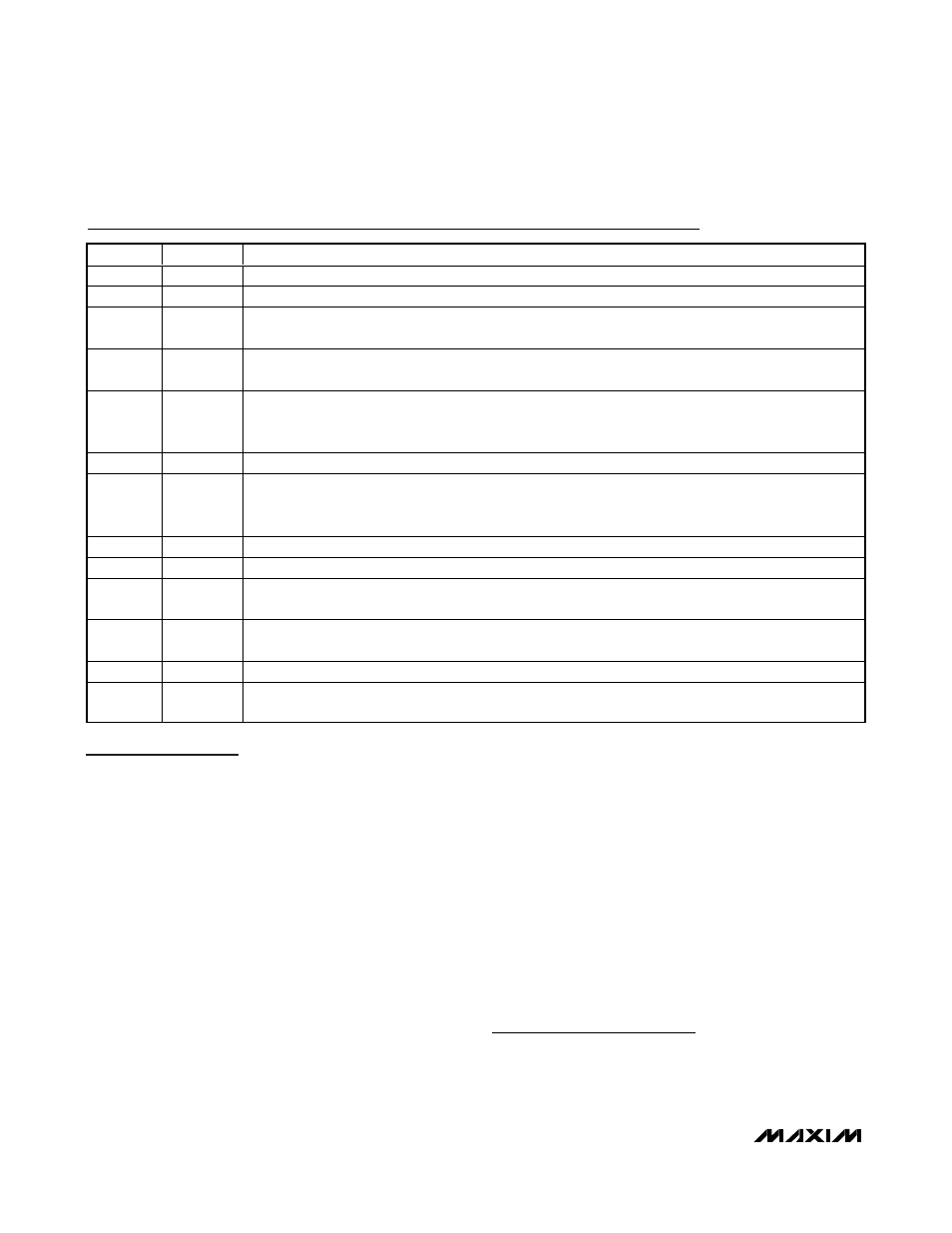
Pin Description
PIN
NAME
FUNCTION
1
SCLK/SCL
Serial Clock Input. Connect SCL to V
DD
through a 2.4k
Ω resistor in I
2
C mode.
2
DIN/SDA
Serial Data Input. Connect SDA to V
DD
through a 2.4k
Ω resistor in I
2
C mode.
3
CS/A0
Chip-Select Input in SPI Mode/Address Select 0 in I
2
C Mode. CS is an active-low input. Connect A0 to
V
DD
or GND to set the device address in I
2
C mode.
4
SPI/I2C
SPI/I2C Select Input. Connect SPI/I2C to V
DD
to select SPI mode, or connect SPI/I2C to GND to select
I
2
C mode.
5
DOUT/A1
Serial Data Output in SPI Mode/Address Select 1 in I
2
C Mode. Use DOUT to daisy chain the MAX5548 to
other devices or to read back in SPI mode. The digital data is clocked out on SCLK’s falling edge.
Connect A1 to V
DD
or GND to set the device address in I
2
C mode.
6, 13, 15
N.C.
No Connection. Leave unconnected or connect to GND.
7
REFIN
Reference Input. Drive REFIN with an external reference source between +0.5V and +1.5V. Leave REFIN
unconnected in internal reference mode. Bypass REFIN with a 0.1µF capacitor to GND as close to the
device as possible.
8, 16
GND
Ground
9
OUTB
DACB Output. OUTB provides up to 30mA of output current.
10
FSADJB
D AC B Ful l - S cal e Ad j ust Inp ut. For m axi m um ful l - scal e outp ut cur r ent, connect a 20k
Ω r esi stor b etw een
FS AD JB and G N D . For m i ni m um ful l - scal e cur r ent, connect a 40k
Ω r esi stor b etw een FS AD JB and G N D .
11
FSADJA
D AC A Ful l - S cal e Ad j ust Inp ut. For m axi m um ful l - scal e outp ut cur r ent, connect a 20k
Ω r esi stor b etw een
FS AD JA and G N D . For m i ni m um ful l - scal e cur r ent, connect a 40k
Ω r esi stor b etw een FS AD JA and G N D .
12
OUTA
DACA Output. OUTA provides up to 30mA of output current.
14
V
DD
Power-Supply Input. Connect V
DD
to a +2.7 to +5.25V power supply. Bypass V
DD
to GND with a 0.1µF
capacitor as close to the device as possible.