Rainbow Electronics MAX15011 User Manual
Page 18
MAX15009/MAX15011
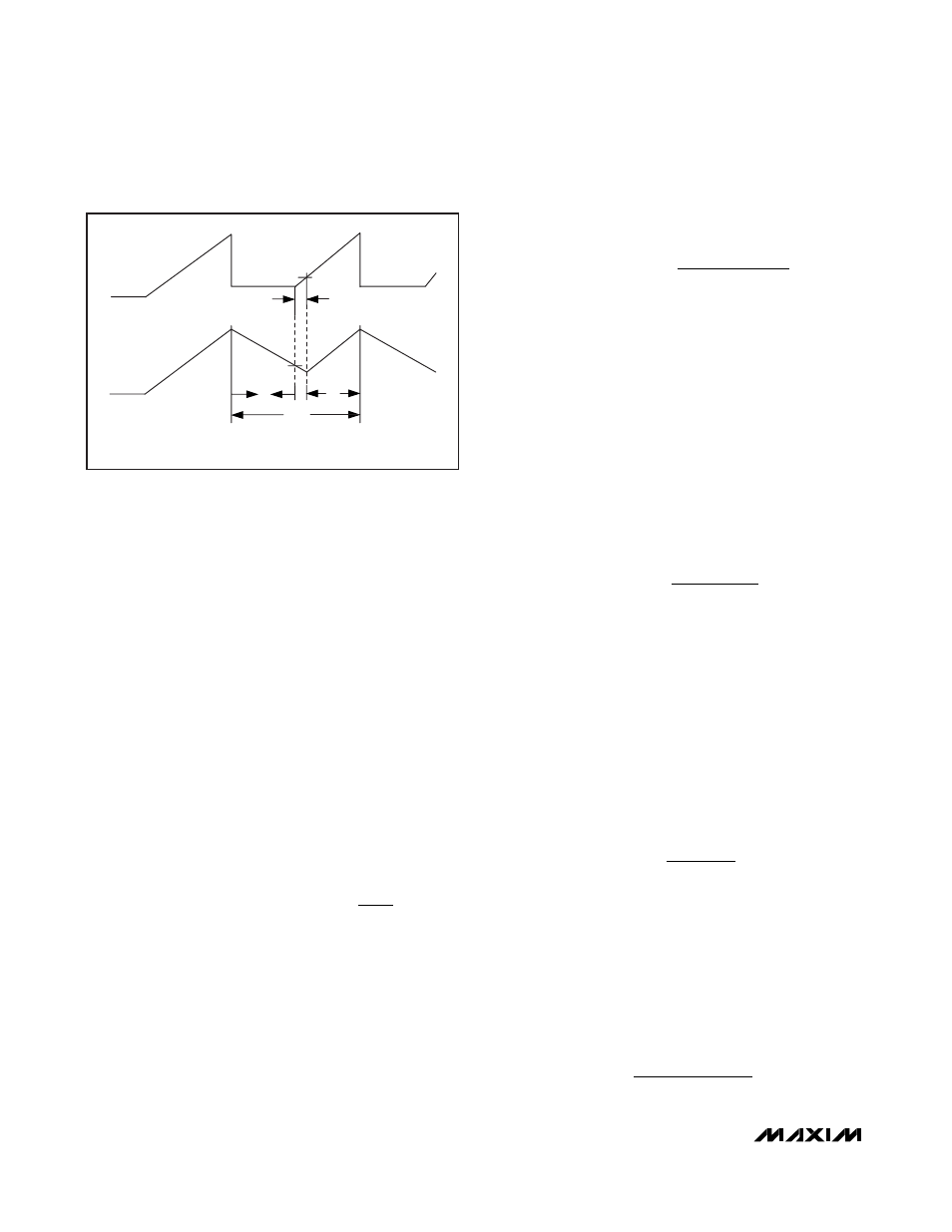
Overvoltage-Limiter Mode
Switching Frequency
When the MAX15009 is configured in overvoltage-
limiter mode, the external n-channel MOSFET is subse-
quently switched on and off during an overvoltage
event. The output voltage at OUT_PROT resembles a
periodic sawtooth waveform. Calculate the period of
the waveform, t
OVP
, by summing three time intervals
(Figure 7):
t
OVP
= t
1
+ t
2
+ t
3
where t
1
is the V
SOURCE
output discharge time, t
2
is the
GATE delay time, and t
3
is the V
SOURCE
output charge
time.
During an overvoltage event, the power dissipated
inside the MAX15009 is due to the gate pulldown cur-
rent, I
GATEPD
. This amount of power dissipation is
worse when I
SOURCE
= 0 (C
SOURCE
is discharged only
by the internal current sink).
The worst-case internal power dissipation contribution
in overvoltage limiter mode, P
OVP
, in watts can be
approximated using the following equation:
where V
OV
is the overvoltage threshold voltage in volts
and I
GATEPD
is 100mA (max) GATE pulldown current.
Output Discharge Time (t
1
)
When the voltage at SOURCE exceeds the adjusted
overvoltage threshold, GATE’s internal pulldown is
enabled until V
SOURCE
drops by 4%. The internal cur-
rent sink, I
GATEPD
, and the external load current,
I
LOAD
, discharge the external capacitance from
SOURCE to ground.
Calculate the discharge time, t
1
, using the following
equation:
where t
1
is in ms, V
OV
is the adjusted overvoltage
threshold in volts, I
LOAD
is the external load current in
mA, and I
GATEPD
is the 100mA (max) internal pulldown
current of GATE. C
SOURCE
is the value of the capacitor
connected between the source of the MOSFET and
PGND in µF.
GATE Delay Time (t
2
)
When SOURCE falls 4% below the overvoltage-threshold
voltage, the internal current sink is disabled and the
internal charge pump begins recharging the external
GATE voltage. Due to the external load, the SOURCE
voltage continues to drop until the gate of the MOSFET is
recharged. The time needed to recharge GATE and re-
enhance the external MOSFET is approximately:
where t
2
is in µs, C
iss
is the input capacitance of the
MOSFET in pF, and V
GS(TH)
is the GATE-to-SOURCE
threshold voltage of the MOSFET in volts. V
F
is the 0.7V
(typ) internal clamp diode forward voltage of the MOS-
FET in volts, and I
GATE
is the charge-pump current
45µA (typ). Any external capacitance between GATE
and PGND adds up to C
iss
.
During t
2
, the SOURCE capacitance, C
SOURCE
, loses
charge through the output load. The voltage across
C
SOURCE
, ΔV
2
, decreases until the MOSFET reaches
its V
GS(TH)
threshold. Approximate ΔV
2
using the fol-
lowing formula:
SOURCE Output Charge Time (t
3
)
Once the GATE voltage exceeds the GATE-to-SOURCE
threshold, V
GS(TH)
, of the external MOSFET, the MOS-
FET turns on and the charge through the internal
charge pump with respect to the drain potential, Q
G
,
determines the slope of the output voltage rise. The
time required for the SOURCE voltage to rise again to
the overvoltage threshold is:
t
C
V
I
rss
SOURCE
GATE
3
=
× Δ
ΔV
I
t
C
LOAD
SOURCE
2
2
=
×
t
C
V
V
I
iss
GS TH
F
GATE
2
=
×
+
(
)
t
C
0.04
V
I
I
1
SOURCE
OV
LOAD
GATEPD
=
Ч
Ч
+
P
V
I
t
t
OVP
OV
GATEPD
OVP
=
Ч
Ч
Ч
0 98
1
.
Automotive 300mA LDO Regulators with
Switched Output and Overvoltage Protector
18
______________________________________________________________________________________
t
2
t
1
t
OVP
t
3
GATE
SOURCE
Figure 7. MAX15009 Timing Diagram