Rainbow Electronics MAX8902B User Manual
Page 7

The BYP capacitor value can be adjusted from 0.001µF
to 0.1µF to change the startup slew rate according to
the following formula:
Startup slew rate = (5V / ms) x (0.01µF / C
BYP
)
Note that this slew rate applies only at startup, and that
recovery from a short circuit occurs at a slew rate
approximately 500 times slower.
Also note that, being a low-frequency filter node, BYP is
sensitive to leakage. BYP leakage currents above 10nA
cause measurable inaccuracy at the output and should
be avoided.
Protection Features
The MAX8902A/MAX8902B are fully protected from an
output short circuit by a current-limiting and thermal-
overload circuit. If the output is shorted to GND, the
output current is limited to 700mA (typ). Under these
conditions, the part quickly heats up. When the junction
temperature reaches +165°C, a thermal-limit circuit
shuts off the output device. When the junction cools to
+150°C, the output turns back on in an attempt to
reestablish regulation. While the fault persists, the out-
put current cycles on and off, as the junction tempera-
ture slews between +150°C and +165°C.
The MAX8902A/MAX8902B are also protected against
reverse current when the output voltage is higher than
the input. In the event that extra output capacitance is
used at the output, a power-down transient at the input
would normally cause a large reverse current through a
conventional regulator. The MAX8902A/MAX8902B
include a reverse voltage detector that trips when IN
drops 10mV below OUT, shutting off the regulator and
opening the pMOS body diode connection, preventing
any reverse current.
Thermal Considerations
The MAX8902A/MAX8902B are packaged in an 8-pin,
2mm x 2mm TDFN package with an exposed paddle.
The exposed paddle is the main path for heat to leave
the IC, and therefore, must be connected to a ground
plane with thermal vias to allow heat to dissipate from
the device. Thermal properties of the IC package are
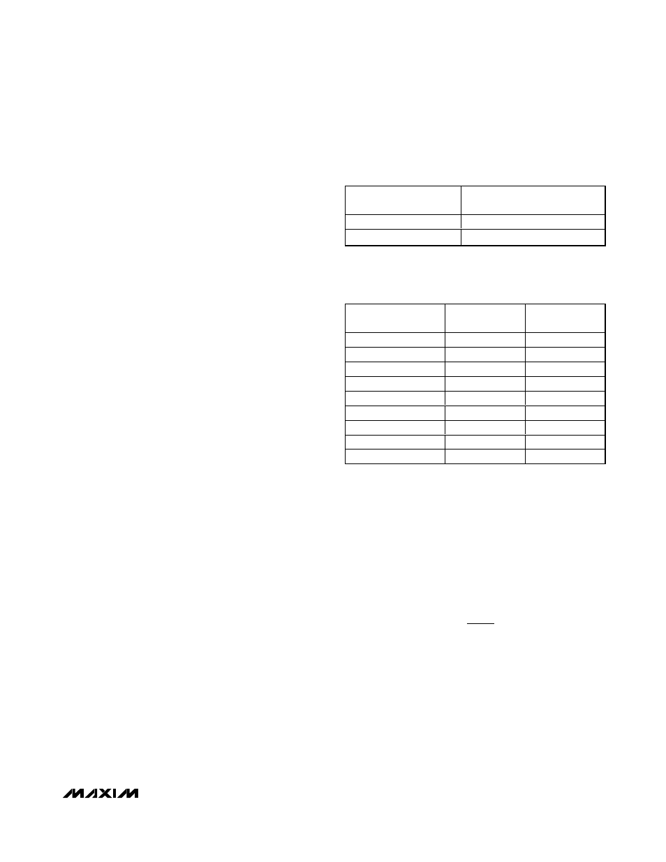
given in Table 1.
Selecting the Output Voltage (MAX8902A)
The MAX8902A output can be set to one of nine volt-
ages by shorting or opening the SELA and SELB
inputs, as shown in Table 2. SELA and SELB should be
connected to GND, IN, or left unconnected.
Alternatively, they may be driven high, low, or open with
external logic; however, the states of SELA and SELB
are sampled only at startup. The regulation voltage can
be set to a different level by cycling EN or IN momen-
tarily to GND.
Setting the Output Voltage (MAX8902B)
The MAX8902B uses external feedback resistors to set
the output regulation voltage as shown in Figure 3. The
output can be set from 0.6V to 5.3V. Set the lower feed-
back resistor (R2) to 120k
Ω or less to minimize FB input
bias current error. Then calculate the value of the upper
feedback resistor (R1) as follows:
where V
FB
is the feedback regulation voltage of 0.6V.
Power-OK (MAX8902B)
The MAX8902B includes an additional open-drain out-
put, POK, that pulls low to indicate the output voltage is
in regulation. During startup, POK is high impedance
until the output voltage rises to 91% of its regulation
level. If an overload occurs at the output, or the output
is shut down, POK is high impedance.
R
R
V
V
OUT
FB
1
2
1
=
×
−
⎛
⎝⎜
⎞
⎠⎟
MAX8902A/MAX8902B
Low-Noise 500mA LDO Regulators
in a 2mm x 2mm TDFN Package
_______________________________________________________________________________________
7
CONTINUOUS POWER
DISSIPATION
953.5mW DERATE 11.9mW/°C
ABOVE +70°C
θ
JA
*
83.9°C/W
θ
JC
36.6°C/W
Table 1. 2mm x 2mm TDFN Package
Thermal Characteristics
OUTPUT VOLTAGE
(V)
SELA STATE
SELB STATE
1.5
IN
Unconnected
1.8
Unconnected
GND
2.0
Unconnected
IN
2.5
Unconnected
Unconnected
3.0
GND
GND
3.1
GND
IN
3.3
GND
Unconnected
4.6
IN
GND
4.7
IN
IN
Table 2. MAX8902A Output Voltages
*
θ
JA
is specified according to the JESD51 standard with the
part mounted on a multilayer PCB.
