Pin configuration pin description – Rainbow Electronics MAX14806 User Manual
Page 7
________________________________________________________________________________________ _ 7
MAX14805/MAX14806
16-Channel (Two Banks of 8-Channel),
High-Voltage Analog Switches
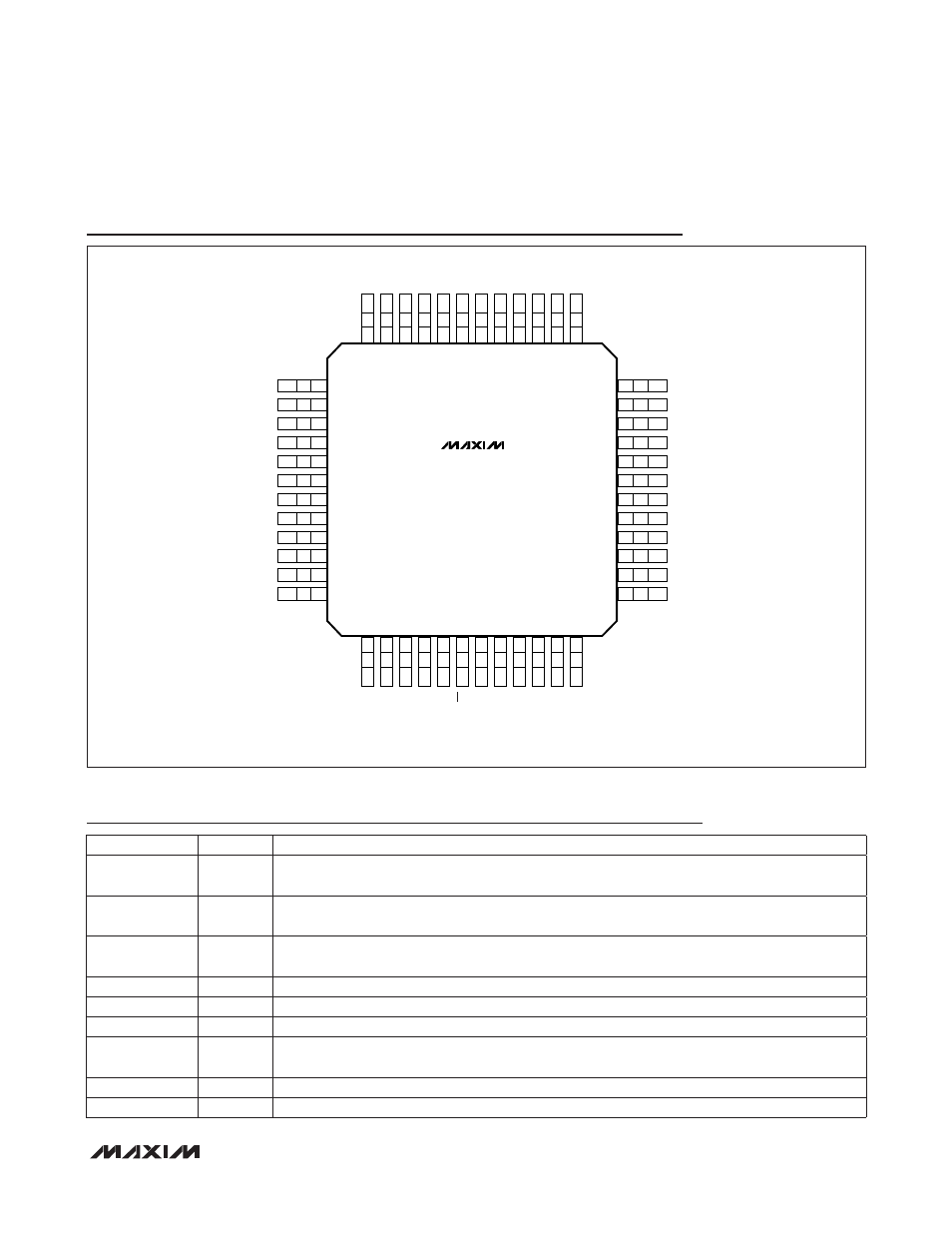
Pin Configuration
Pin Description
TQFP
(7mm × 7mm × 1.4mm)
TOP VIEW
+
MAX14805
MAX14806
1
2
3
4
5
6
7
8
9
10
11
12
V
NN
N.C.
V
PP
N.C.
DIN1
LE
DIN2
N.C.
N.C.
V
DD
GND
N.C.
36
35
34
33
32
31
30
29
28
27
26
25
SW5
SW5
SW6
SW6
SW7
SW7
SW8
SW8
SW9
SW9
SW10
SW10
37
38
39
40
41
42
43
44
45
46
47
48
SW4
N.C.
SW4
N.C.
SW3
SW3
SW2
SW2
SW1
SW1
SW0
SW0
24
23
22
21
20
19
18
17
16
15
14
13
N.C.
SW11
SW11
SW12
SW12
SW13
SW13
SW14
SW14
SW15
SW15
N.C.
PIN
NAME
FUNCTION
1
V
NN
Negative High-Voltage Power Supply. Bypass V
NN
to GND with a 0.1FF or greater ceramic
capacitor as close as possible to the device.
2, 4, 8, 9, 12,
13, 24, 38, 40
N.C.
No Connection. Not internally connected.
3
V
PP
Positive High-Voltage Power Supply. Bypass V
PP
to GND with a 0.1FF or greater ceramic capac-
itor as close as possible to the device.
5
DIN1
Data Input 1
6
LE
Active-Low Latch Enable Input. Drive LE low to latch data input. Drive LE high to hold data.
7
DIN2
Data Input 2
10
V
DD
Digital Power Supply. Bypass V
DD
to GND with a 0.1FF or greater ceramic capacitor as close as
possible to the device.
11
GND
Ground
14, 15
SW15
Analog Switch Terminal 15