Table 3. bipolar code table, Bipolar output, Using an ac reference – Rainbow Electronics MAX5159 User Manual
Page 14: Harmonic distortion and noise
MAX5158/MAX5159
produce a range of 0V to 2.5V with a 1.25V reference.
Table 2 lists the unipolar output codes. An offset to the
output can be achieved by connecting a voltage to
OS_, as shown in Figure 10. By applying V
OS
_ = -1V,
the output values will range between 1V and (1V +
V
REF
x 2).
Bipolar Output
The MAX5158/MAX5159 can be configured for a bipo-
lar output, as shown in Figure 11. The output voltage is
given by the equation (OS_ = AGND):
V
OUT
= V
REF
[((2 x NB) / 1024) - 1]
where NB represents the numeric value of the DAC’s
binary input code. Table 3 shows digital codes and the
corresponding output voltage for Figure 11’s circuit.
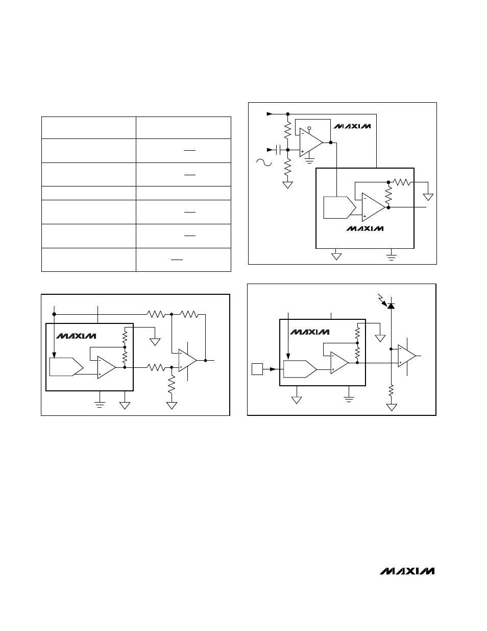
Using an AC Reference
In applications where the reference has an AC signal
component, the MAX5158/MAX5159 have multiplying
capabilities within the reference input voltage range
specifications. Figure 12 shows a technique for apply-
ing a sinusoidal input to REF_, where the AC signal is
offset before being applied to the reference input.
Harmonic Distortion and Noise
The total harmonic distortion plus noise (THD+N) is typ-
ically less than -78dB at full scale with a 1Vp-p input
swing at 5kHz. The typical -3dB frequency is 300kHz
for both devices, as shown in the
Typical Operating
Characteristics.
Low-Power, Dual, 10-Bit Voltage-Output DACs
with Serial Interface
14
______________________________________________________________________________________
Table 3. Bipolar Code Table
ANALOG OUTPUT
1 1
1 1 1 1
1 1 1 1 ( 0 0 0 )
1 0
0 0 0 0
0 0 0 1 ( 0 0 0 )
DAC CONTENTS
MSB
LSB
1 0
0 0 0 0
0 0 0 0 ( 0 0 0 )
0V
0 1
1 1 1 1
1 1 1 1 ( 0 0 0 )
0 0
0 0 0 0
0 0 0 0 ( 0 0 0 )
0 0
0 0 0 0
0 0 0 1 ( 0 0 0 )
+V
511
512
REF
+V
1
512
REF
-V
1
512
REF
-V
511
512
REF
-V
512
512
- V
REF
REF
=
AGND
DGND
R
R
MAX5158
MAX5159
DAC _
REF_
OS_
OUT_
10k
10k
10k
10k
V-
V+
V
DD
V
OUT
+5V/+3V
Figure 11. Bipolar Output Circuit
DAC_
OUT_
MAX5158
MAX5159
10k
26k
OS_
REF
R
R
V
DD
DGND
AGND
+5V/
+3V
AC
REFERENCE
INPUT
500mVp-p
MAX495
+5V/+3V
Figure 12. AC Reference Input Circuit
AGND
DIN
µ
P
DGND
MAX5158
MAX5159
DAC _
REF_
OS_
OUT_
R
R
V-
V+
PHOTODIODE
V+
V
DD
V
OUT
R
PULLDOWN
+5V/+3V
Figure 13. Digital Calibration
Note:
( ) are for the sub bits.