Detailed description – Rainbow Electronics MAX5183 User Manual
Page 8
MAX5180/MAX5183
Dual, 10-Bit, 40MHz, Current/Voltage
Simultaneous-Output DACs
8
_______________________________________________________________________________________
Detailed Description
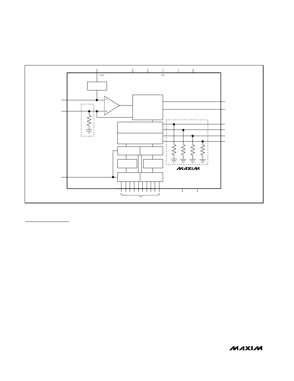
The MAX5180/MAX5183 are dual, 10-bit digital-to-ana-
log converters (DACs) capable of operating with clock
speeds up to 40MHz. Each of these dual converters
consists of separate input and DAC registers, followed
by a current source array capable of generating up to
1.5mA full-scale output current (Figure 1). An integrat-
ed +1.2V voltage reference and control amplifier deter-
mine the data converters’ full-scale output currents/
voltages. Careful reference design ensures close gain
matching and excellent drift characteristics. The
MAX5183’s voltage output operation features matched
400
Ω on-chip resistors that convert the current array
current into a voltage.
Internal Reference and Control Amplifier
The MAX5180/MAX5183 provide an integrated
50ppm/°C, +1.2V, low-noise bandgap reference that
can be disabled and overridden by an external refer-
ence voltage. REFO serves either as an external refer-
ence input or an integrated reference output. If REN is
connected to AGND, the internal reference is selected
and REFO provides a +1.2V output. Due to its limited
10µA output drive capability, REFO must be buffered
with an external amplifier, if heavier loading is required.
The MAX5180/MAX5183 also employ a control amplifier
designed to simultaneously regulate the full-scale out-
put current (I
FS
) for both outputs of the devices. The
output current is calculated as follows:
I
FS
= 8
× I
REF
where I
REF
is the reference output current (I
REF
=
V
REFO/
R
SET
) and I
FS
is the full-scale output current.
R
SET
is the reference resistor that determines the
amplifier’s output current on the MAX5180 (Figure 2).
This current is mirrored into the current-source array
where it is equally distributed between matched current
segments and summed to valid output current readings
for the DACs.
The MAX5183 converts each output current (DAC1 and
DAC2) into an output voltage (V
OUT1
, V
OUT2
) with two
internal, ground-referenced 400
Ω load resistors. Using
the internal +1.2V reference voltage, the MAX5183’s
integrated reference output current resistor (R
SET
=
9.6k
Ω) sets I
REF
to 125µA and I
FS
to 1mA.
9.6k
REFR
REFO
1.2V REF
REN
CURRENT-
SOURCE ARRAY
DAC 1 SWITCHES
DAC 2 SWITCHES
400
Ω
MSB DECODE
CLK
OUTPUT
LATCHES
OUTPUT
LATCHES
MSB DECODE
*INTERNAL 400
Ω AND 9.6kΩ
RESISTORS FOR MAX5183 ONLY.
AV
DD
AGND
DACEN
PD
*
*
*
*
DV
DD
DGND
D9–D0
CS
CREF2
MAX5180
MAX5183
CREF1
OUT2P
OUT1P
OUT2N
OUT1N
400
Ω
400
Ω
400
Ω
INPUT
LATCHES
INPUT
LATCHES
*
Figure 1. Functional Diagram