Design procedure, Table 1. protection features – Rainbow Electronics MAX8575 User Manual
Page 8
MAX8570–MAX8575
High-Efficiency LCD Boost
with True Shutdown
8
_______________________________________________________________________________________
Design Procedure
Inductor Selection
Smaller inductance values typically offer smaller physi-
cal size for a given series resistance or saturation cur-
rent. Circuits using larger inductance values may
provide more output power. The inductor’s saturation
current rating should be greater than the peak switch-
ing current. Recommended inductor values range from
10µH to 100µH.
Selecting the Current Limit
The peak LX current limit (I
LX(MAX)
) required for the
application is calculated from the following equation:
where P
OUT(MAX)
is the maximum output power
required by the load and V
BATT(MIN)
is the minimum
supply voltage used to supply the inductor (this is V
CC
unless a separate supply is used for the inductor). The
IC current limit must be greater than this calculated
value. See the Selector Guide on page 1 for selecting
the IC with the correct current limit.
Diode Selection
The high switching frequency of up to 800kHz requires
a high-speed rectifier. Schottky diodes are recom-
mended due to their low forward-voltage drop. To
maintain high efficiency, the average current rating of
the diode should be greater than the peak switching
current. Choose a reverse breakdown voltage greater
than the output voltage.
Capacitors
Small ceramic surface-mount capacitors with X7R or
X5R temperature characteristics are recommended
due to their small size, low cost, low equivalent series
resistance (ESR), and low equivalent series inductance
(ESL). If nonceramic capacitors are used, it is important
that they have low ESR to reduce the output ripple volt-
age and peak-peak load-transient voltage.
For most applications, use a 1µF ceramic capacitor for
the output and V
CC
bypass capacitors. For SW or the
inductor supply, a 4.7µF or greater ceramic capacitor
is recommended.
I
P
V
P
V
s
P
L
LX MAX
OUT MAX
BATT MIN
OUT MAX
BATT MIN
OUT MAX
(
)
(
)
(
)
(
)
(
)
(
)
.
.
≥
Ч
+
Ч
+ µ ×
1 25
1 25
3
2
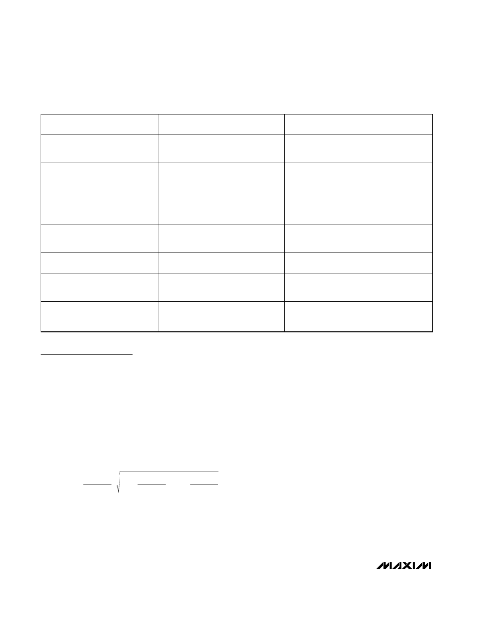
COMMON APPLICATION FAULTS
RESULT WITH COMPETING
STEP-UP CONVERTERS
RESULT WITH MAX8570 FAMILY
OUT to FB resistor missing or
disconnected.
OUT voltage rises until the output
capacitor is destroyed and/or
downstream components are damaged.
Converter stops switching.
Output cap missing and FB floating.
OUT voltage rises until the output
capacitor is destroyed and/or
downstream components are damaged.
LX may boost one or two times before the FB
voltage exceeds the trip point. In the rare case
where the capacitive loading and external
loading on OUT is small enough that the energy
in one cycle can slew it more than 50V, the
internal MOSFET will clamp between 35V and
70V (nondestructively).
FB shorted to GND.
OUT voltage rises until the output
capacitor is destroyed and/or
downstream components are damaged.
Converter stops switching and OUT is resistively
loaded to GND.
Diode missing or disconnected.
Diode reverse polarity.
Inductor energy forces LX node high,
possibly damaging the internal switch.
OUT is resistively loaded to GND and the
converter stops switching.
FB node floating.
Unpredictable, possibly boosting output
voltage beyond acceptable design
range.
FB node driven above its regulation point, the
converter stops switching, and OUT is resistively
loaded to GND.
OUT shorted to ground.
Current ramps up through inductor and
diode, generally destroying one of the
devices.
True off-switch detects short, opens when
current reaches pMOS current limit, and restarts
soft-start. This protects the inductor and diode.
Table 1. Protection Features