Preliminary w78c51d – Rainbow Electronics W78C51D User Manual
Page 3
Preliminary W78C51D
Publication Release Date: January 1999
- 3 -
Revision A1
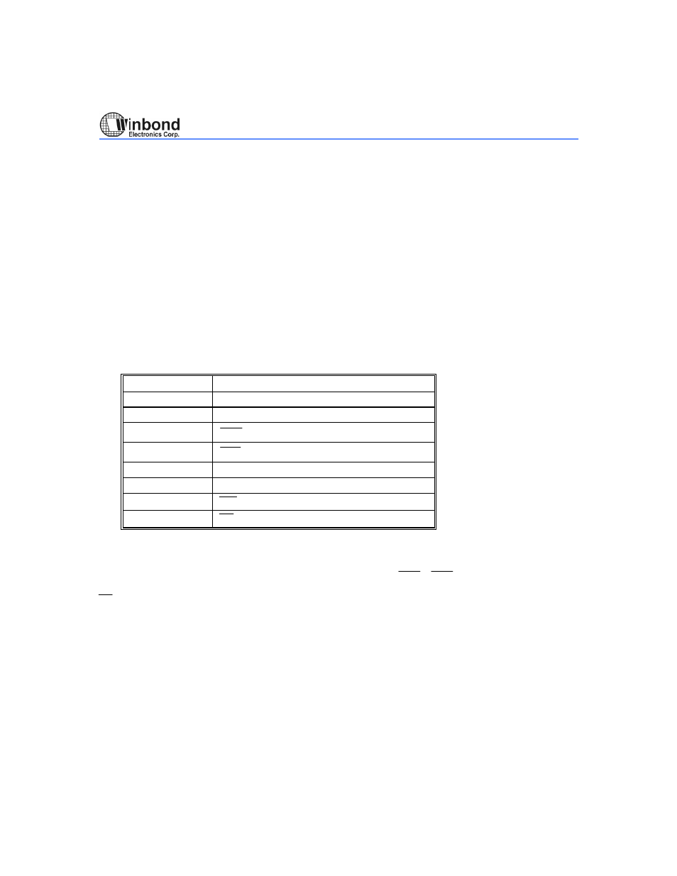
PIN DESCRIPTION
P0.0
−P0.7
Port 0, Bits 0 through 7. Port 0 is a bidirectional I/O port. This port also provides a multiplexed low
order address/data bus during accesses to external memory.
P1.0
−P1.7
Port 1, Bits 0 through 7. Port 1 is a bidirectional I/O port with internal pull-ups.
P2.0
−P2.7
Port 2, Bits 0 through 7. Port 2 is a bidirectional I/O port with internal pull-ups. This port also provides
the upper address bits for accesses to external memory.
P3.0
−P3.7
Port 3, Bits 0 through 7. Port 3 is a bidirectional I/O port with internal pull-ups. All bits have alternate
functions, which are described below:
PIN
ALTERNATE FUNCTION
P3.0
RXD Serial Receive Data
P3.1
TXD Serial Transmit Data
P3.2
INT0 External Interrupt 0
P3.3
INT1 External Interrupt 1
P3.4
T0 Timer 0 Input
P3.5
T1 Timer 1 Input
P3.6
WR Data Write Strobe
P3.7
RD Data Read Strobe
P4.0
−P4.3
Another bit-addressable bidirectional I/O port P4. P4.3 and P4.2 are alternative function pins. It can
be used as general I/O pins or external interrupt input sources (
INT2
/ INT3 ).
EA
External Address Input, active low. This pin forces the processor to execute out of external ROM.
This pin should be kept low for all W78C31 operations.
RST
Reset Input, active high. This pin resets the processor. It must be kept high for at least two machine
cycles in order to be recognized by the processor.
ALE
Address Latch Enable Output, active high. ALE is used to enable the address latch that separates the
address from the data on Port 0. ALE runs at 1/6th of the oscillator frequency. A single ALE pulse is
skipped during external data memory accesses. ALE goes to a high impedance state during reset with
a weak pull-up.