Preliminary w78c51d – Rainbow Electronics W78C51D User Manual
Page 11
Preliminary W78C51D
Publication Release Date: January 1999
- 11 -
Revision A1
AC CHARACTERISTICS
The AC specifications are a function of the particular process used to manufacture the part, the
ratings of the I/O buffers, the capacitive load, and the internal routing capacitance. Most of the
specifications can be expressed in terms of multiple input clock periods (T
CP
), and actual parts will
usually experience less than a
±20 nS variation. The numbers below represent the performance
expected from a 0.5 micron CMOS process when using 2 and 4 mA output buffers.
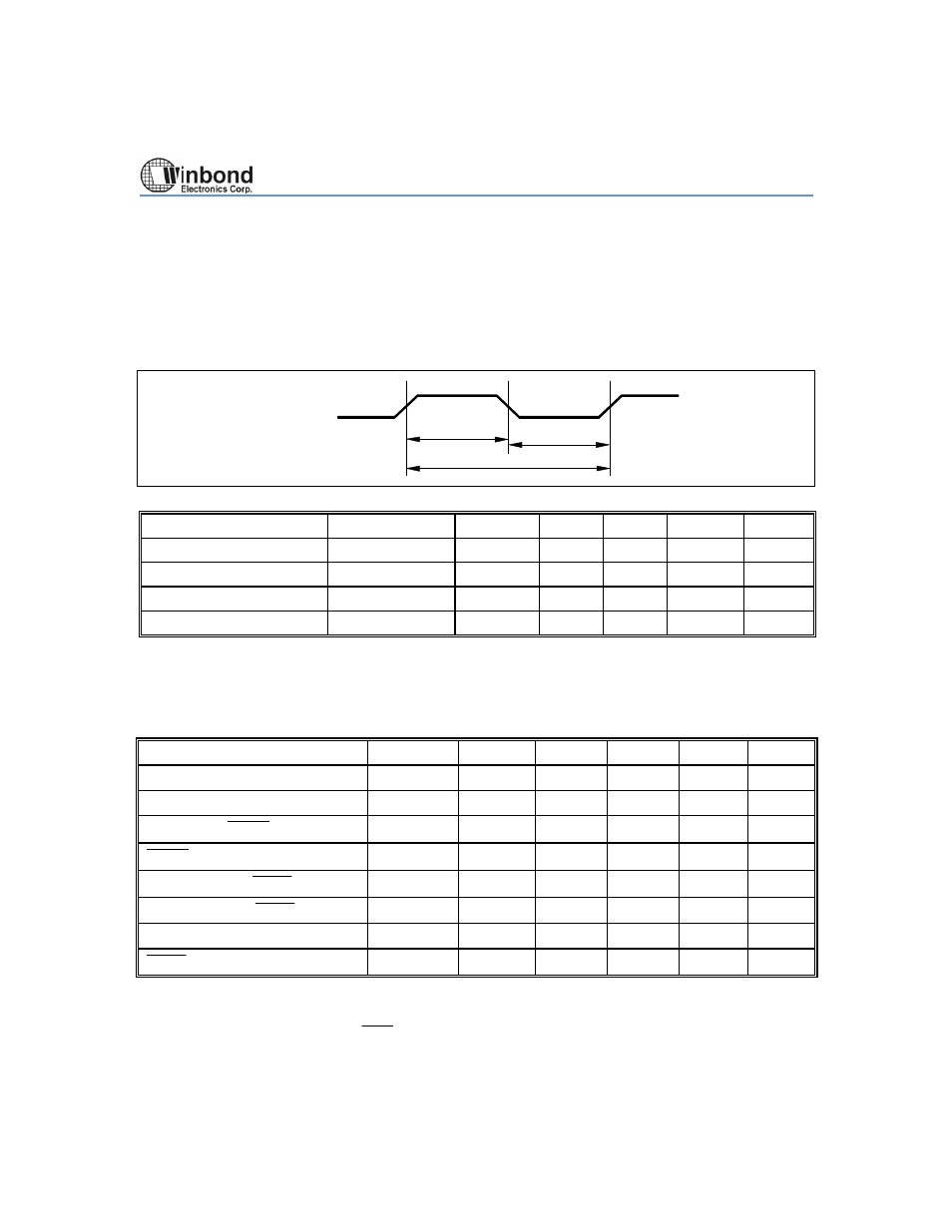
Clock Input Waveform
T
T
XTAL1
F
CH
CL
OP,
T
CP
PARAMETER
SYMBOL
MIN.
TYP.
MAX.
UNIT
NOTES
Operating Speed
F
OP
0
-
40
MHz
1
Clock Period
T
CP
25
-
-
nS
2
Clock High
T
CH
10
-
-
nS
3
Clock Low
T
CL
10
-
-
nS
3
Notes:
1. The clock may be stopped indefinitely in either state.
2. The T
CP
specification is used as a reference in other specifications.
3. There are no duty cycle requirements on the XTAL1 input.
Program Fetch Cycle
PARAMETER
SYMBOL
MIN.
TYP.
MAX.
UNIT
NOTES
Address Valid to ALE Low
T
AAS
1 T
CP
-
∆
-
-
nS
4
Address Hold from ALE Low
T
AAH
1 T
CP
-
∆
-
-
nS
1, 4
ALE Low to
PSEN Low
T
APL
1 T
CP
-
∆
-
-
nS
4
PSEN Low to Data Valid
T
PDA
-
-
2 T
CP
nS
2
Data Hold after PSEN High
T
PDH
0
-
1 T
CP
nS
3
Data Float after PSEN High
T
PDZ
0
-
1 T
CP
nS
ALE Pulse Width
T
ALW
2 T
CP
-
∆
2 T
CP
-
nS
4
PSEN Pulse Width
T
PSW
3 T
CP
-
∆
3 T
CP
-
nS
4
Notes:
1. P0.0
−P0.7, P2.0−P2.7 remain stable throughout entire memory cycle.
2. Memory access time is 3 T
CP
.
3. Data have been latched internally prior to PSEN going high.
4. "
∆" (due to buffer driving delay and wire loading) is 20 nS.