Bypass fet for wcdma and cdmaone handsets, Detailed description, Pin description – Rainbow Electronics MAX8508 User Manual
Page 6
MAX8506/MAX8507/MAX8508
PWM Step-Down DC-DC Converters with 75m
Ω
Bypass FET for WCDMA and cdmaOne Handsets
6
_______________________________________________________________________________________
Detailed Description
The MAX8506/MAX8507/MAX8508 PWM step-down DC-
DC converters with integrated bypass PFET are opti-
mized for low-voltage, battery-powered applications
where high efficiency and small size are priorities. An
analog control signal dynamically adjusts the MAX8506/
MAX8507s’ output voltage from 0.4V to 3.4V with a set-
tling time of 30µs. The MAX8508 uses external feedback
resistors to set the output voltage from 0.75V to 3.4V.
The MAX8506/MAX8507/MAX8508 operate at a high
1MHz switching frequency that reduces external com-
ponent size. Each device includes an internal synchro-
nous rectifier for high efficiency, which eliminates the
need for an external Schottky diode. The normal operat-
ing mode uses constant-frequency PWM switching at
medium and heavy loads and automatically pulse skips
at light loads to reduce supply current and extend bat-
tery life. A forced-PWM mode switches at a constant
frequency, regardless of load, to provide a well-con-
trolled spectrum in noise-sensitive applications. Battery
life is maximized by the low-dropout (75mΩ) high-
power mode and a 0.1µA (typ) logic-controlled shut-
down mode.
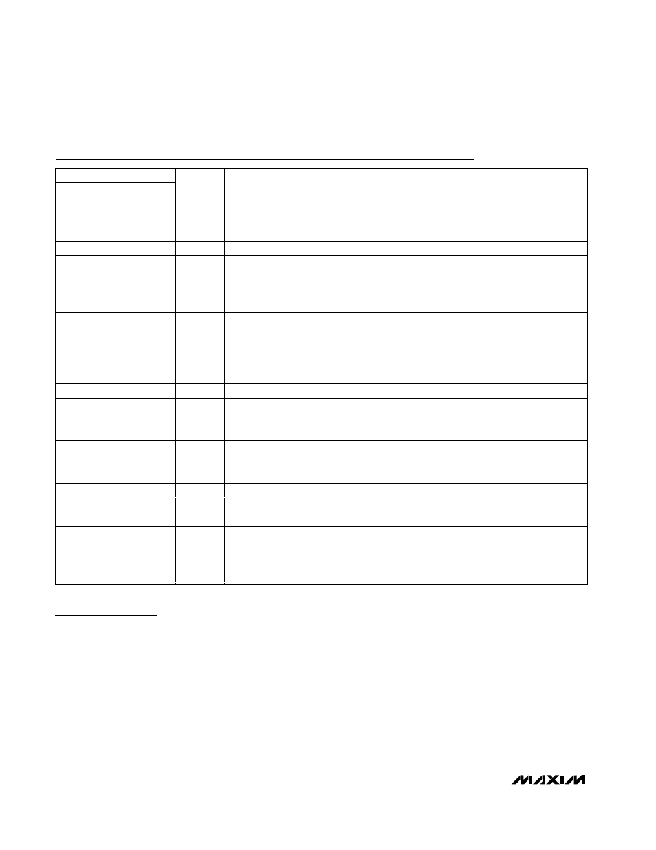
Pin Description
PIN
MAX8506
MAX8507
MAX8508
NAME
FUNCTION
1
1
SHDN
Shutdown Control Input. Drive low for shutdown mode. Connect to BATT or logic high to
enable the IC.
2
2
GND
Ground. Connect to PGND and directly to EP.
3
3
REF
Reference Output. Output of the internal 1.25V reference. Bypass to GND with a 0.22µF
capacitor.
4
—
REFIN
External Reference Input. Connect to the output of a digital-to-analog converter for
dynamic adjustment of the output voltage.
5
5
COMP
Compensation. Connect a compensation network from COMP to GND to stabilize the
regulator. See the Typical Application Circuits.
6
6
HP
High-Power Bypass Control Input. Drive low for OUT to regulate to the voltage set by
REFIN (MAX8506/MAX8507) or the external resistors on FB (MAX8508). Drive HP high for
OUT to be connected to BATT by an internal bypass PFET.
7
7
N.C.
No Connection. Connect to PGND.
8
8
PGND
Power Ground. Connect to GND.
9
9
LX
Inductor Connection to the Drains of the Internal Power MOSFETs. LX is high impedance
in shutdown mode.
10
10
BATTP
Supply Voltage Input. Connect to a 2.6V to 5.5V source. Bypass BATTP to PGND with a
low-ESR 2.2µF capacitor. Connect BATTP to BATT.
11, 13, 15
11, 13, 15
BATT
Supply Voltage Input. Connect all BATT pins to BATTP.
12, 14
12, 14
OUT
Regulator Output. Connect both OUT pins directly to the output voltage.
16
16
SKIP
Skip Control Input. Connect to GND or drive low to enable pulse skipping under light
loads. Connect SKIP to BATT or logic high for forced-PWM mode.
—
4
FB
Output Feedback Sense Input. To set the output voltage, connect FB to the center of an
external resistive voltage-divider between OUT and GND. FB voltage regulates to 0.75V
when HP is low.
—
—
EP
Exposed Pad. Connect directly to GND underneath the IC.