Bypass fet for wcdma and cdmaone handsets, Absolute maximum ratings, Electrical characteristics – Rainbow Electronics MAX8508 User Manual
Page 2
MAX8506/MAX8507/MAX8508
PWM Step-Down DC-DC Converters with 75m
Ω
Bypass FET for WCDMA and cdmaOne Handsets
2
_______________________________________________________________________________________
ABSOLUTE MAXIMUM RATINGS
Stresses beyond those listed under “Absolute Maximum Ratings” may cause permanent damage to the device. These are stress ratings only, and functional
operation of the device at these or any other conditions beyond those indicated in the operational sections of the specifications is not implied. Exposure to
absolute maximum rating conditions for extended periods may affect device reliability.
BATTP, BATT, OUT,
SHDN, SKIP, HP, REFIN,
FB to GND ...........................................................-0.3V to +6V
PGND to GND .......................................................-0.3V to +0.3V
BATT to BATTP......................................................-0.3V to +0.3V
OUT, COMP, REF to GND.......................-0.3V to (V
BATT
+ 0.3V)
LX Current (Note 1) ...............................................................1.6A
OUT Current (Note 1)............................................................3.2A
Output Short-Circuit Duration.....................................Continuous
Continuous Power Dissipation (T
A
= +70°C)
16-Pin Thin QFN (derate 16.9mW/°C above +70°C) ...1.349W
Operating Temperature Range ...........................-40°C to +85°C
Junction Temperature ......................................................+150°C
Storage Temperature Range .............................-65°C to +150°C
Lead Temperature (soldering, 10s) .................................+300°C
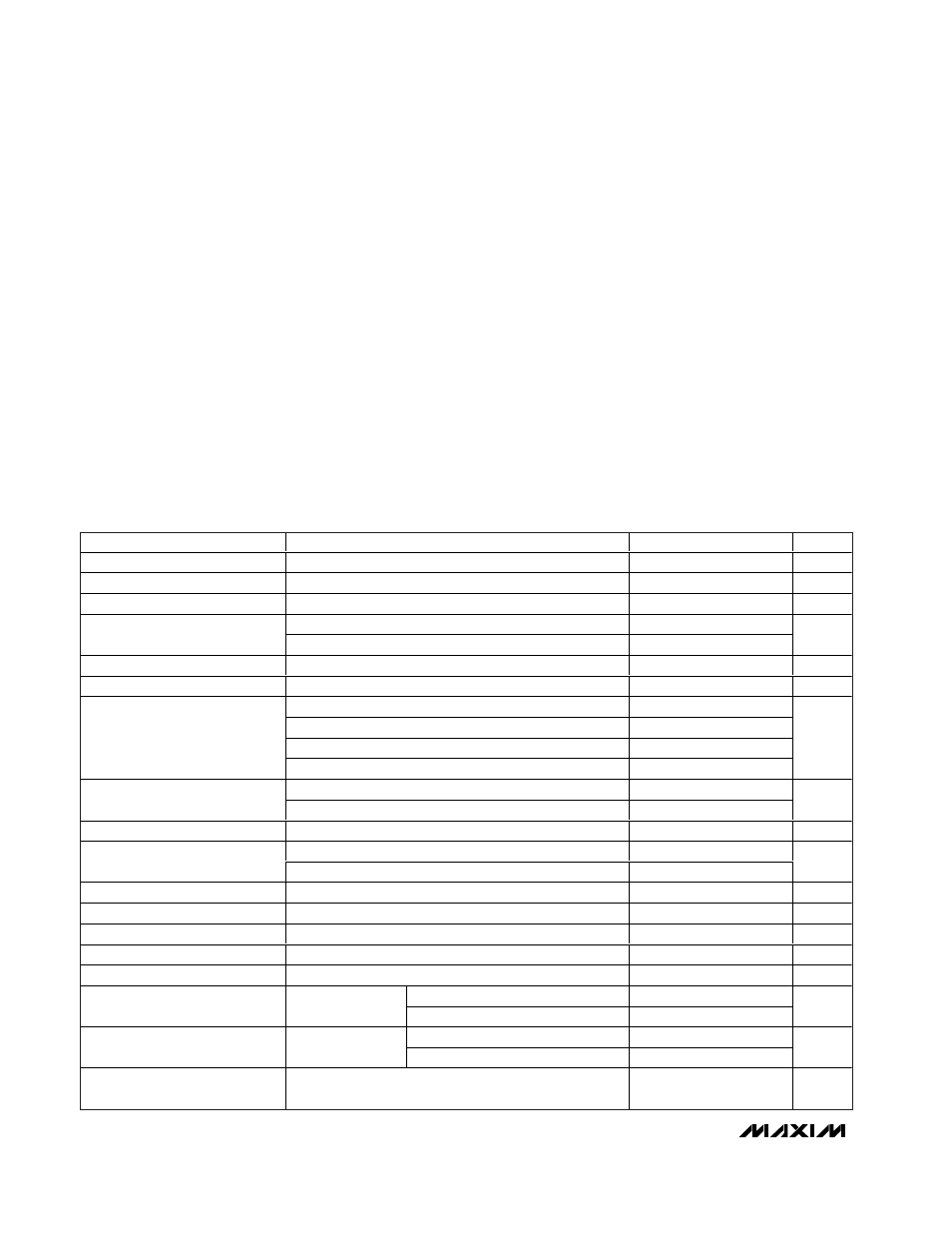
ELECTRICAL CHARACTERISTICS
(V
BATT
= V
BATTP
= 3.6V, SHDN = SKIP = BATT, HP = GND, V
REFIN
= 1.932V (MAX8506), V
REFIN
= 1.70V (MAX8507),
C
REF
= 0.22µF, T
A
= -40°C to +85°C, unless otherwise noted. Typical values are at T
A
= +25°C.) (Note 2)
PARAMETER
CONDITIONS
MIN
TYP
MAX
UNITS
Input BATT Voltage
2.6
5.5
V
Undervoltage Lockout Threshold
V
BATT
rising
2.150
2.35
2.575
V
Undervoltage Lockout Hysteresis
40
mV
SKIP = GND (normal mode)
180
250
Quiescent Current
SKIP = BATT, 1MHz switching
1750
µA
Quiescent Current in Dropout
HP = BATT
775
1000
µA
Shutdown Supply Current
SHDN = GND
0.1
5
µA
V
REFIN
= 1.932V, I
OUT
= 0 to 600mA (MAX8506)
3.375
3.40
3.425
V
REFIN
= 0.426V, I
OUT
= 0 to 30mA (MAX8506)
0.740
0.75
0.760
V
REFIN
= 1.700V, I
OUT
= 0 to 600mA (MAX8507)
3.375
3.40
3.425
OUT Voltage Accuracy
V
REFIN
= 0.375V, I
OUT
= 0 to 30mA (MAX8507)
0.740
0.75
0.760
V
MAX8506
250
485
OUT Input Resistance
MAX8507
275
535
k
Ω
REFIN Input Current
-1
0.1
+1
µA
MAX8506
1.76
REFIN to OUT Gain
MAX8507
2.00
V/V
Reference Voltage
1.225
1.25
1.275
V
Reference Load Regulation
10µA < I
REF
< 100µA
2.5
8.5
mV
Reference Bypass Capacitor
0.1
0.22
µF
FB Voltage Accuracy
FB = COMP (MAX8508)
0.7275
0.75
0.7725
V
FB Input Current
V
FB
= 1V (MAX8508)
0.03
0.175
µA
V
BATT
= 3.6V
0.4
0.825
P-Channel On-Resistance
I
LX
= 180mA
V
BATT
= 2.6V
0.5
Ω
V
BATT
= 3.6V
0.3
0.5
N-Channel On-Resistance
I
LX
= 180mA
V
BATT
= 2.6V
0.35
Ω
HP/Bypass P-Channel
On-Resistance
I
OUT
= 180mA, V
BATT
= 3.6V
0.075
0.110
Ω
Note 1: LX has internal clamp diodes to PGND and BATT. Applications that forward bias these diodes should take care not to exceed
the IC’s package power-dissipation limits.