Detailed description, Internal reference – Rainbow Electronics MAX5131 User Manual
Page 9

MAX5130/MAX5131
+3V/+5V, 13-Bit, Serial Voltage-Output DACs
with Internal Reference
_______________________________________________________________________________________
9
_______________Detailed Description
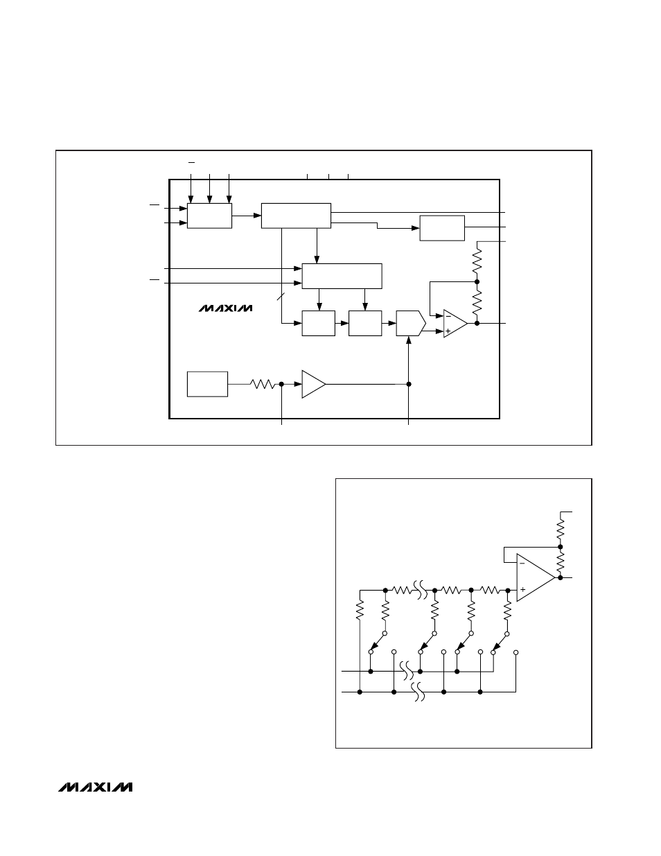
The MAX5130/MAX5131 13-bit, voltage-output DACs
are easily configured with a 3-wire serial interface. They
include a 16-bit data-in/data-out shift register and have
a double-buffered input consisting of an input register
and a DAC register. In addition, these devices employ
precision bandgap references and trimmed internal
resistors to produce a gain of 1.6384V/V, maximizing
the output voltage swing (Figure 1). The MAX5130/
MAX5131 output amplifier’s offset-adjust pin allows for
a DC shift in the DAC outputs. The full-scale output volt-
age is +4.0955V for the MAX5130 and +2.04775V for
the MAX5131. These DACs are designed with an invert-
ed R-2R ladder network (Figure 2) that produces a
weighted output voltage proportional to the digital input
code.
Internal Reference
Both the MAX5130 and MAX5131 use an on-board pre-
cision bandgap reference to generate an output volt-
age of +2.5V (MAX5130) or +1.25V (MAX5131). With a
low temperature coefficient of only 10ppm/°C (max),
the REF pin can source up to 100µA and may become
unstable with capacitive loads exceeding 100pF.
REFADJ can be used for minor adjustments (1%) to the
MAX5130
MAX5131
SR
CONTROL
16-BIT
SHIFT REGISTER
DECODE
CONTROL
INPUT
REGISTER
BANDGAP
REFERENCE
REFERENCE
BUFFER
DAC
REGISTER
DAC
2X
(1X)
DOUT
UPO
OUT
OS
R
0.6384R
GAIN = 1.6384X
4k
1.25V
AGND DGND
V
DD
DIN SCLK
CS
2.5V, (1.25V)
LOGIC
OUTPUT
CLR
PDL
PD
RSTVAL
REFADJ
REF
13
( ) FOR MAX5131 ONLY
Figure 1. Simplified Functional Block Diagram
OUT
OS
R
0.6384R
SHOWN FOR ALL 1s ON DAC
*INTERNAL 2.5V (MAX5130) AND 1.25V (MAX5131) OR EXTERNAL REFERENCE.
D0 D10
D11
D12
2R
2R
2R
2R
2R
R
R
R
REF*
AGND
Figure 2. Simplified Inverted R-2R DAC Structure
