Applications information – Rainbow Electronics MAX7407 User Manual
Page 10

V
DD
V
SUPPLY
IN
CLK
GND
INPUT
OUTPUT
50k
50k
50k
OUT
0.1
µ
F
0.1
µ
F
0.1
µ
F
CLOCK
SHDN
COM
OS
MAX7400
MAX7403
MAX7404
MAX7407
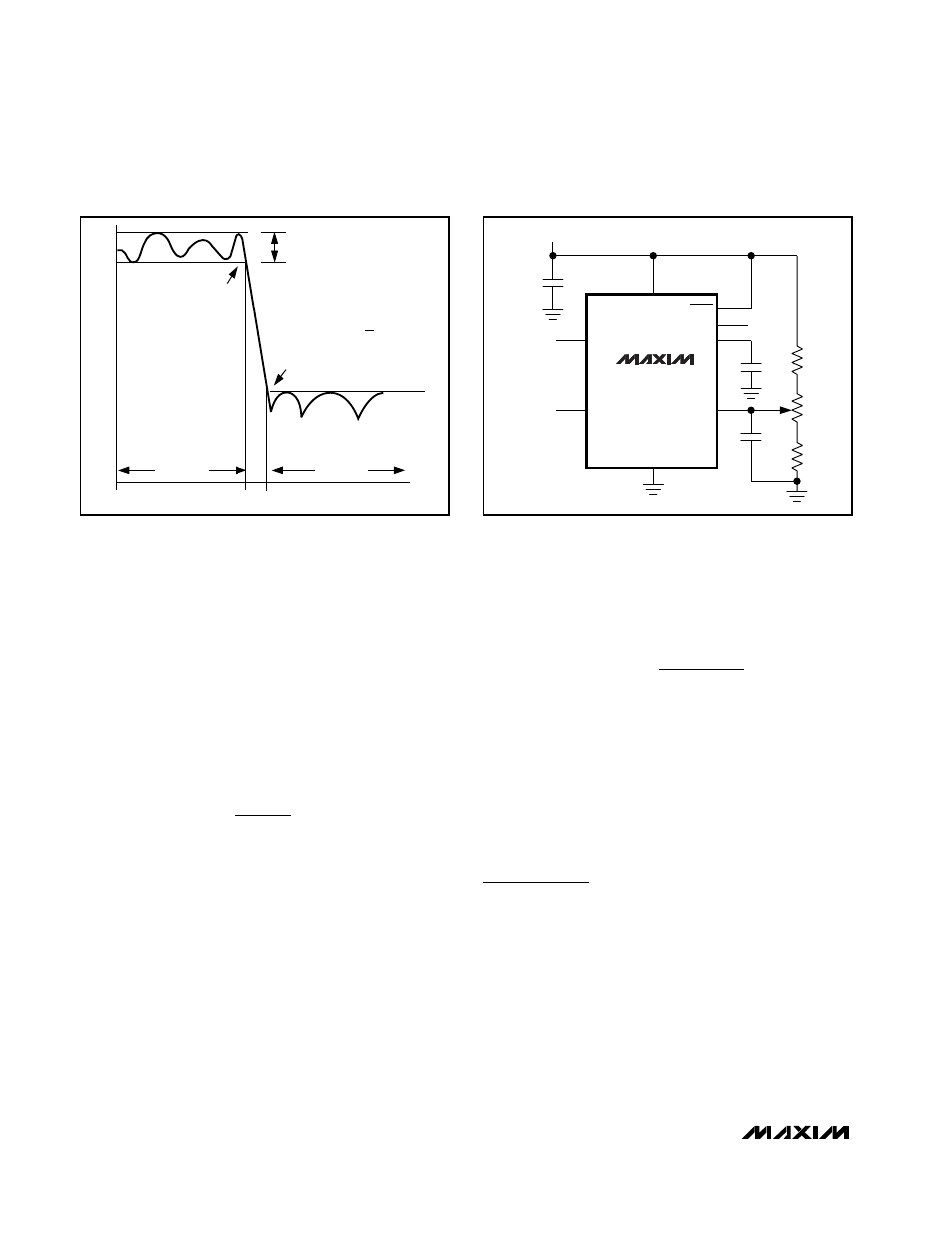
Figure 4. Offset Adjustment Circuit
MAX7400/MAX7403/MAX7404/MAX7407
8th-Order, Lowpass, Elliptic,
Switched-Capacitor Filters
10
______________________________________________________________________________________
Clock Signal
External Clock
The MAX7400/MAX7403/MAX7404/MAX7407 SCFs
were designed for use with external clocks that have a
40% to 60% duty cycle. When using an external clock,
drive CLK with a CMOS gate powered from 0 to V
DD
.
Varying the rate of the external clock adjusts the filter
corner frequency:
f
C
= f
CLK
/ 100
Internal Clock
When using the internal oscillator, the capacitance
(C
OSC
) on the CLK pin determines the oscillator fre-
quency:
where K = 38 for the MAX7400/MAX7403, and K = 34
for the MAX7404/MAX7407. Since the capacitor value
is in picofarads, minimize the stray capacitance at CLK
so that it does not affect the internal oscillator frequen-
cy. Varying the rate of the internal oscillator adjusts the
filter’s corner frequency by a 100:1 clock-to-corner fre-
quency ratio. For example, an internal oscillator fre-
quency of 100kHz produces a nominal corner
frequency of 1kHz.
Input Impedance
vs. Clock Frequencies
The MAX7400/MAX7403/MAX7404/MAX7407’s input
impedance is effectively that of a switched-capacitor
resistor and is inversely proportional to frequency. The
input impedance determined by the following equation
represents the average input impedance, since the
input current is not continuous. As a rule, use a driver
with an output source impedance less than 10% of the
filter’s input impedance. Estimate the input impedance
of the filter using the following formula:
where f
CLK
= clock frequency and C
IN
= 0.85pF.
Low-Power Shutdown Mode
These devices feature a shutdown mode that is activat-
ed by driving SHDN low. Placing the filter in shutdown
mode reduces the supply current to 0.2µA (typ) and
places the output of the filter into a high-impedance
state. For normal operation, drive SHDN high or con-
nect to V
DD
.
Applications Information
Offset and Common-Mode
Input Adjustment
The voltage at COM sets the common-mode input volt-
age and is internally biased at midsupply by a resistor-
divider. Bypass COM with a 0.1µF capacitor and
connect OS to COM. For applications requiring offset
adjustment or DC level shifting, apply an external bias
voltage through a resistor-divider network to OS, as
shown in Figure 4. (Note: Do not leave OS unconnect-
ed.) The output voltage is represented by the following
equation:
V
OUT
= (V
IN
- V
COM
) + V
OS
Z
f
C
IN
CLK
IN
( )
(
)
Ω =
⋅
1
f
(kHz) =
K 10
C
OSC
3
OSC
⋅
;
C
in pF
OSC
PASSBAND
STOPBAND
GAIN (dB)
FREQUENCY
f
C
f
S
f
S
f
C
f
S
f
C
TRANSITION RATIO =
RIPPLE
Figure 3. Elliptic Filter Response
