Timing circuits/timing diagrams (continued), Pin description – Rainbow Electronics MAX4885 User Manual
Page 8
MAX4885
Complete VGA 1:2 or 2:1 Multiplexer
8
_______________________________________________________________________________________
Timing Circuits/Timing Diagrams (continued)
MEASUREMENTS ARE STANDARDIZED AGAINST SHORTS AT IC TERMINALS.
OFF-ISOLATION IS MEASURED BETWEEN R0 AND R1 OR R2 ON EACH SWITCH.
ON-LOSS IS MEASURED BETWEEN R0 AND R1 OR R2 ON EACH SWITCH.
CROSSTALK IS MEASURED FROM ONE CHANNEL TO THE OTHER CHANNEL.
SIGNAL DIRECTION THROUGH SWITCH IS REVERSED; WORST VALUES ARE RECORDED.
+5V
V
OUT
V+
SEL
V
IN
MAX4885
OFF-ISOLATION = 20log
✕
V
OUT
V
IN
ON-LOSS = 20log
✕
V
OUT
V
IN
CROSSTALK = 20log
✕
V
OUT
V
IN
NETWORK
ANALYZER
50
Ω
50
Ω
50
Ω
50
Ω
MEAS
REF
10nF
0V OR V+
50
Ω
GND
R0, G0, B0
R2, G2, B2
R1, G1, B1
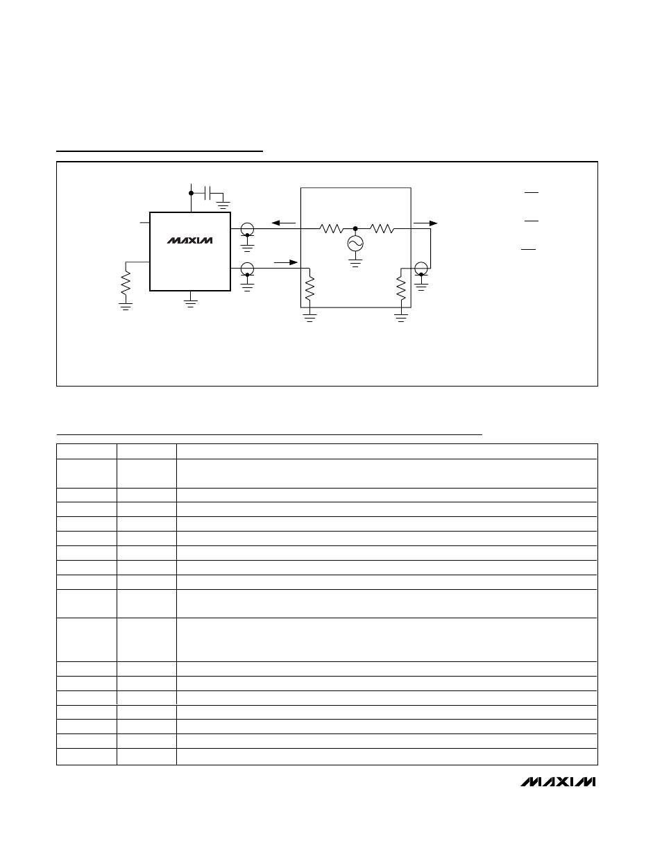
Figure 4. On-Loss, Off-Isolation, and Crosstalk
Pin Description
PIN
NAME
FUNCTION
1
QP
Charge-Pump Enable, Active Low. Drive QP low for normal operation. Drive QP high to disable the
internal charge pump.
2
R0
RGB Analog I/O
3
G0
RGB Analog I/O
4
B0
RGB Analog I/O
5
H0
Horizontal Sync I/O
6
V0
Vertical Sync I/O
7
DDCA0
DDC I/O
8
DDCB0
DDC I/O
9
EN
Enable Input, Active Low. Drive EN low for normal operation. Drive EN high to disable the device. All
I/Os are high-impedance and charge pump is off when the device is disabled.
10
V
CL
DDC Clamp Voltage. Open-drain DDCA_ and DDCB_ outputs are clamped to one diode-drop below
V
CL
. +2.7V < V
CL
< V+. Connect V
CL
to +3.3V for voltage clamping, or connect to V+ to disable
clamping. Bypass V
CL
to GND with a 0.1µF or larger ceramic capacitor.
11, 21, 30
V+
Supply Voltage. V+ = +5.0V ± 10%. Bypass each to GND with a 0.1µF or larger ceramic capacitor.
12, 20, 29
GND
Ground
13
DDCA2
DDC I/O
14
DDCB2
DDC I/O
15
R2
RGB Analog I/O
16
G2
RGB Analog I/O
17
B2
RGB Analog I/O