Absolute maximum ratings, Electrical characteristics – Rainbow Electronics MAX4885 User Manual
Page 2
MAX4885
Complete VGA 1:2 or 2:1 Multiplexer
2
_______________________________________________________________________________________
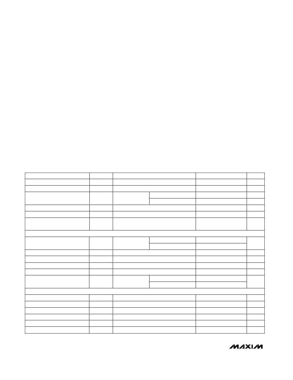
ABSOLUTE MAXIMUM RATINGS
Stresses beyond those listed under “Absolute Maximum Ratings” may cause permanent damage to the device. These are stress ratings only, and functional
operation of the device at these or any other conditions beyond those indicated in the operational sections of the specifications is not implied. Exposure to
absolute maximum rating conditions for extended periods may affect device reliability.
(All voltages referenced to GND.)
V
+
, V
CL
.....................................................................-0.3V to +6V
R_, G_, B_, DDCA_, DDCB_, SEL, M,
EN, QP (Note 1) ...........................................-0.3V to V+ + 0.3V
H_, V_ .......................................................................-0.3V to +6V
Continuous Current Through RGB Switches ....................±70mA
Continuous Current Through HV, DDC Switches…..........±50mA
Peak Current Through RGB Switches
(pulsed at 1ms, 10% duty cycle).................................±140mA
Peak Current Through HV, DDC Switches (pulsed at 1ms,
10% duty cycle)..............................................................±100mA
Continuous Power Dissipation (T
A
= +70°C)
32-Pin TQFN (derate 21.3mW/°C above +70°C) ........1702mW
Operating Temperature Range ...........................-40°C to +85°C
Storage Temperature Range .............................-65°C to +150°C
Junction Temperature ......................................................+150°C
Lead Temperature (soldering, 10s) .................................+300°C
ELECTRICAL CHARACTERISTICS
(V+ = +5.0V ±10%, V
CL
= +3.3V ±10%, T
A
= T
MIN
to T
MAX
, QP = GND, unless otherwise noted. Typical values are at V+ = +5.0V,
V
CL
= +3.3V and T
A
= +25°C.)
PARAMETER
SYMBOL
CONDITIONS
MIN
TYP
MAX
UNITS
Supply Voltage Range
V+
4.5
5.5
V
Clamp Voltage Range
V
CL
2.7
V+
V
QP = GND
0.3
0.5
mA
V
+
Quiescent Supply Current
I
+
V+ = +5.5V
QP = V+
1
µA
V
CL
Quiescent Supply Current
I
CL
V
CL
= V+ = +5.5V
1
µA
V
+
Shutdown Current
I
+SHDN
V+ = +5.5V, all digital inputs to V+ or GND
5
µA
V
CL
Shutdown Current
I
CLSHDN
V
CL
= V+ = +5.5V, all digital inputs to V+ or
GND
1
µA
RGB ANALOG SWITCHES
QP = GND
5
7.5
On-Resistance
R
ON
0V < V
IN
< +2.5V,
I
IN
= -40mA
QP = V+
6
10
Ω
On-Resistance Matching
∆R
ON
0V < V
IN
< +2.5V, I
IN
= -40mA
0.5
1.5
Ω
On-Resistance Flatness
R
FLAT(ON)
0V < V
IN
< +2.5V, I
IN
= -40mA
0.02
0.75
Ω
Off-Leakage Current
I
L(OFF)
R_, G_, B_ = 0V or +5.5V, EN = GND
-1
+1
µA
On-Leakage Current
I
L(ON)
R_, G_, B_ = 0V or +5.5V, EN = V+
-1
+1
µA
QP = GND
10
Charge Injection
Q
R_, G_, B_ = 0V,
C
L
= 1000pF
QP = V+
8
pC
HV MULTIPLEXER
Input-Voltage Low
V
ILHV
M = GND
0.8
V
Input-Voltage High
V
IHHV
M = GND
2.0
V
High-Output Drive Current
I
OHHV
V
OUT
= V
+
- 0.5V, M = GND
-16
mA
Low-Output Drive Current
I
OLHV
V
OUT
= +0.5V, M = GND
+16
mA
On-Resistance
R
ONHV
H_ = V_ = +2.5V, I
IN
= -40mA, M = V+
15
Ω
Charge Injection
Q
H_, V_ = 0V, M = V+, C
L
= 1000pF
21
pC
Note 1: Signals exceeding V+ or GND are clamped by internal diodes. Limit forward-diode current to maximum current rating.