Applications information – Rainbow Electronics MAX8668 User Manual
Page 13
MAX8667/MAX8668
1.5MHz Dual Step-Down DC-DC Converters
with Dual LDOs and Individual Enables
______________________________________________________________________________________
13
Applications Information
Setting the Output Voltages
and Voltage Positioning
The LDO output voltages of the MAX8667/MAX8668,
and the step-down outputs of the MAX8667 are factory
preset. See the
Selector Guide
to find the part number
corresponding to the desired output voltages.
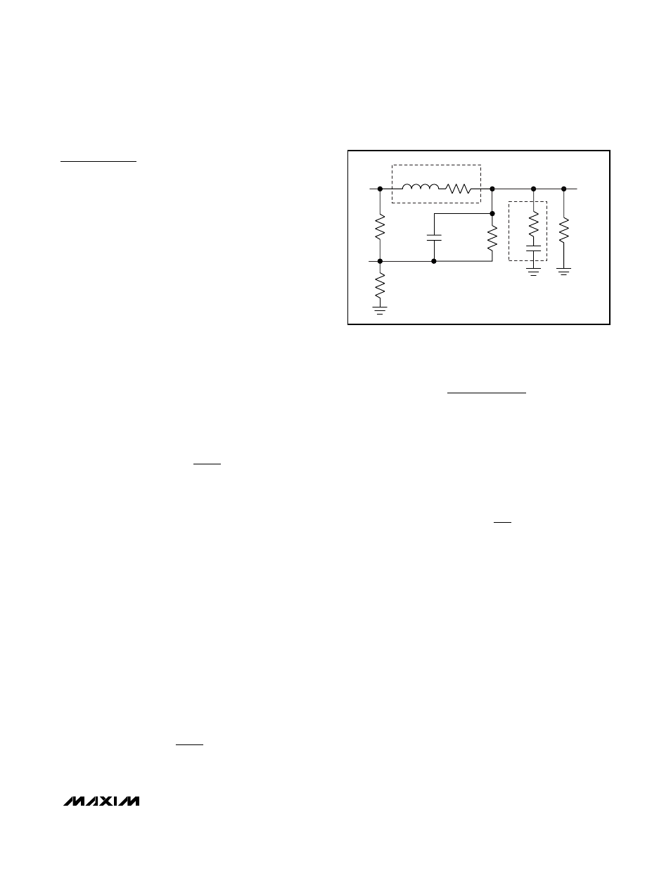
The OUT1 and OUT2 output voltages of the MAX8668
are set by a resistor network connected to FB_ as
shown in Figure 5. With this configuration, a portion of
the feedback signal is sensed on the switched side of
the inductor (LX), and the output voltage droops slightly
as the load current is increased due to the DC resis-
tance of the inductor (DCR). This allows the load regu-
lation to be set to match the voltage droop during a
load transient (voltage positioning), reducing the peak-
to-peak output-voltage deviation during a load tran-
sient, and reducing the output capacitance
requirements.
For the simplest method of setting the output voltage,
R6 is not installed. Choose the value of R2 (a good
starting value is 100kΩ), and then calculate the value of
R1 as follows:
where V
FB
is the feedback regulation voltage (0.6V).
With the voltage set in this manner, the voltage posi-
tioning depends only on the DCR, and the maximum
output voltage droop is:
Setting the Output Voltages with
Reduced Voltage Positioning
To obtain less voltage positioning than described in the
previous section, use the following procedure for set-
ting the output voltages. The OUT1 and OUT2 output
voltages and voltage positioning of the MAX8668 are
set by a resistor network connected to FB_ as shown in
Figure 5.
To set the output voltage (V
OUT
), first select a value for
R2 (a good starting value is 100kΩ). Then calculate the
value of R
EQ
(the equivalent parallel resistance of R1
and R6) as follows:
where V
FB
is the feedback-regulation voltage (0.6V).
Calculate the factor m based on the desired load-regu-
lation improvement:
where I
OUT(MAX)
is the maximum output current, DCR is
the inductor series resistance, and
ΔV
OUT(DESIRED)
is the
maximum allowable droop in the output voltage at full
load. The calculated value for m must be between 1.1 and
2; m = 2 results in a 2x improvement in load regulation.
Now calculate the values of R1 and R6 as follows:
The value of R1 should always be lower than the value
of R6.
Power-Supply Sequencing
The MAX8667/MAX8668 have individual enable inputs
for each regulator to allow complete control over the
power sequencing. When all EN_ inputs are low, the IC
is in low-power shutdown mode, reducing the supply
current to less than 1µA. After one of the EN_ inputs
asserts high, the corresponding regulator begins soft-
start after a delay of t
EN
(see Figure 2). The first output
enabled from shutdown mode or initially powering up
the IC has a longer delay (t
PWRON
) as the IC exits the
low-power shutdown mode.
Inductor Selection
The MAX8667/MAX8668 step-down converters operate
with inductors between 2.2µH and 4.7µH. Low induc-
tance values are physically smaller, but require faster
switching, resulting in some efficiency loss. The induc-
tor’s DC current rating must be high enough to account
R
R
m
R
R
EQ
EQ
m
m
1
6
1
=
Ч
=
Ч
−
m
I
DCR
V
OUT MAX
OUT DESIRED
=
×
(
)
(
)
Δ
R
V
V
R
EQ
OUT
FB
=
−
⎛
⎝⎜
⎞
⎠⎟
×
1
2
ΔV
DCR I
OUT MAX
OUT MAX
(
)
(
)
=
×
R
R
V
V
OUT
FB
1
2
1
=
×
−
⎛
⎝⎜
⎞
⎠⎟
L1
DCR
LX_
FB_
OUT
ESR
C6
R
LOAD
R1
R6
(OPTIONAL)
R2
C4
Figure 5. MAX8668 Feedback Network