Rainbow Electronics MAX6641 User Manual
Page 9
Register Descriptions
Temperature Registers (00h, 01h)
These registers contain the 8-bit results of the tempera-
ture measurements. Register 00h contains the tempera-
ture reading of the remote diode. Register 01h contains
the ambient temperature reading. The value of the MSB
is +128
°C and the value of the LSB is +1°C. The MSB is
transmitted first. The POR state of the temperature reg-
isters is 00h.
Configuration Byte Register (02h)
The configuration byte register controls the timeout
conditions and various PWMOUT signals. The POR
state of the configuration byte register is 00h. See
Table
2 for configuration byte definitions.
Remote and Local
OT
Limits (03h, 04h)
Set the remote (03h) and local (04h) temperature thresh-
olds with these two registers. Once the temperature is
above the threshold, the OT output is asserted low (for
the temperature channels that are not masked). The POR
state of the remote OT limit register is 6Eh and the POR
state of the LOCAL OT limit register is 50h.
OT
Status (05h)
Read the OT status register to determine which channel
recorded an over-temperature condition. Bit D7 is high if
the fault reading occurred from the remote diode. Bit D6
is high if the fault reading occurred in the local diode.
The OT status register is cleared only by reading its con-
tents. Reading the contents of the register also makes
the OT output high impedance. If the fault is still present
on the next temperature measurement cycle, the corre-
sponding bits and the OT output are set again. After
reading the OT status register, a temperature register
read must be done to correctly clear the appropriate sta-
tus bit. The POR state of the OT status register is 00h.
MAX6641
SMBus-Compatible Temperature Monitor with
Automatic PWM Fan-Speed Controller
_______________________________________________________________________________________
9
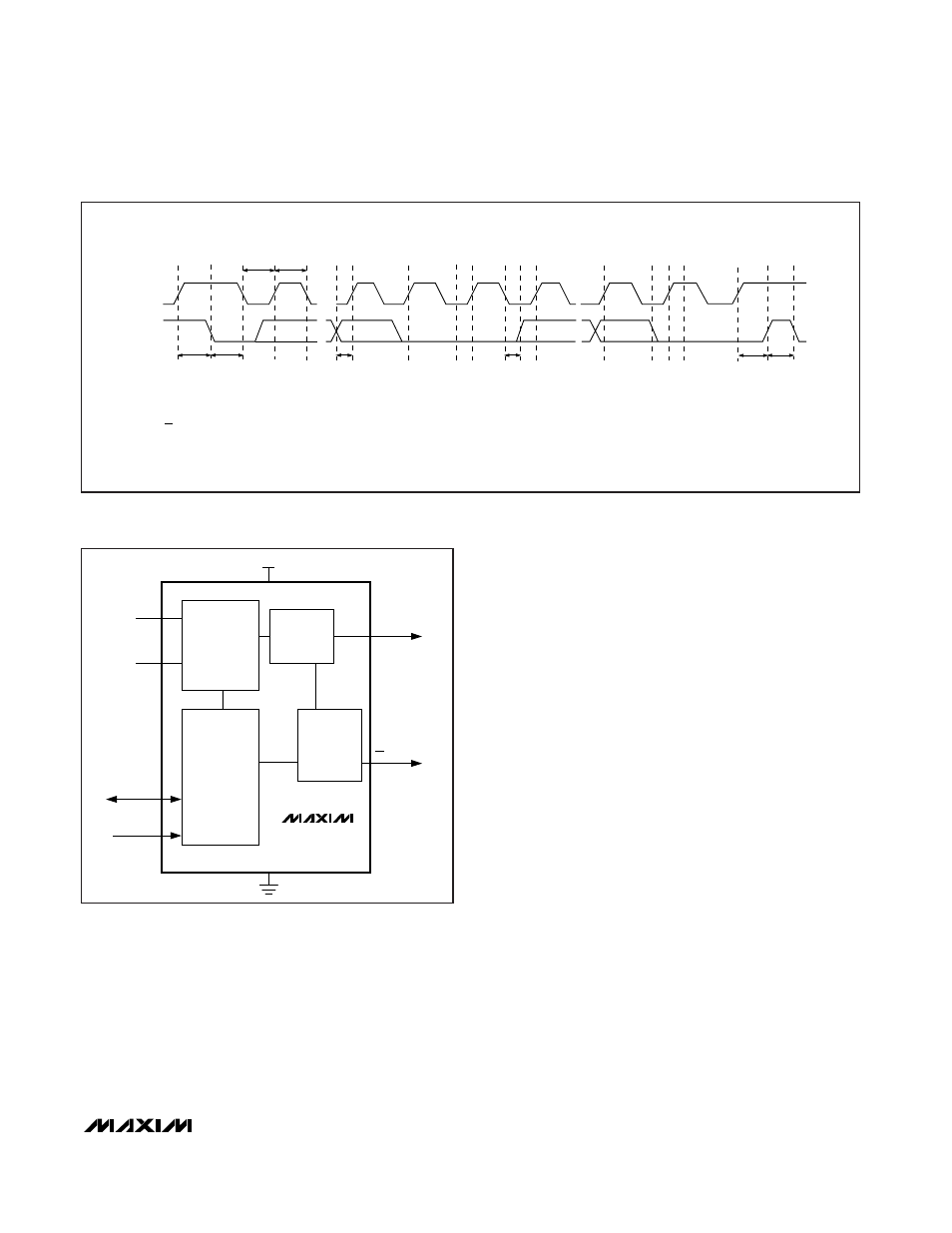
SMBCLK
A
B
C
D
E
F
G
H
I
J
K
SMBDATA
t
SU:STA
t
HD:STA
t
LOW
t
HIGH
t
SU:DAT
t
HD:DAT
t
SU:STO
t
BUF
A = START CONDITION
B = MSB OF ADDRESS CLOCKED INTO SLAVE
C = LSB OF ADDRESS CLOCKED INTO SLAVE
D = R/W BIT CLOCKED INTO SLAVE
E = SLAVE PULLS SMBDATA LINE LOW
L
M
F = ACKNOWLEDGE BIT CLOCKED INTO MASTER
G = MSB OF DATA CLOCKED INTO MASTER
H = LSB OF DATA CLOCKED INTO MASTER
I = MASTER PULLS DATA LINE LOW
J = ACKNOWLEDGE CLOCKED INTO SLAVE
K = ACKNOWLEDGE CLOCK PULSE
L = STOP CONDITION
M = NEW START CONDITION
Figure 3. SMBus Read Timing Diagram
Figure 4. Block Diagram
GND
SMBus
INTERFACE AND
REGISTERS
LOGIC
PWM
GENERATOR
BLOCK
V
CC
TEMPERATURE
PROCESSING
BLOCK
SMBDATA
SMBCLK
DXP
DXN
PWMOUT
OT
MAX6641