Chip information – Rainbow Electronics MAX8614B User Manual
Page 13
MAX8614A/MAX8614B
Dual-Output (+ and -) DC-DC
Converters for CCD
______________________________________________________________________________________
13
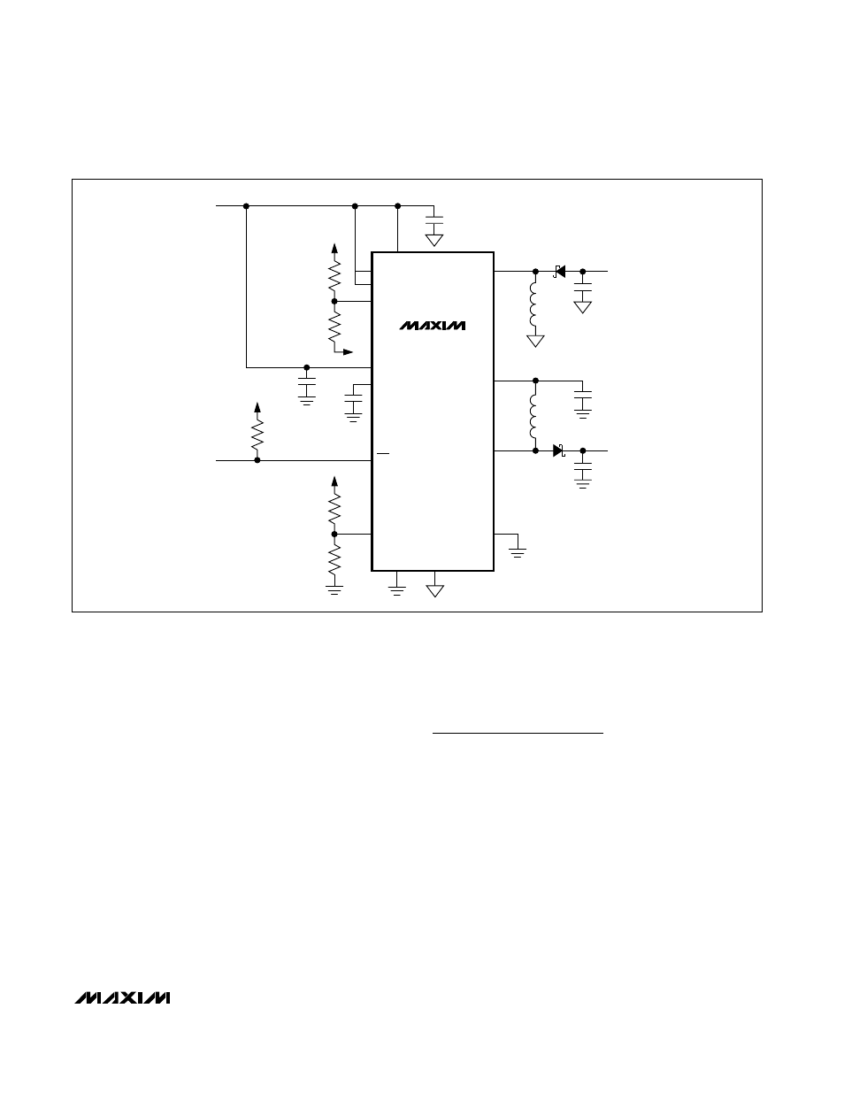
It is important to connect the GND pin, the input
bypass-capacitor ground lead, and the output filter
capacitor ground lead to a single point (star ground
configuration) to minimize ground noise and improve
regulation. Also, minimize lead lengths to reduce stray
capacitance, trace resistance, and radiated noise, with
preference given to the feedback circuit, the ground
circuit, and LX_. Place feedback resistors R1–R4 as
close to their respective feedback pins as possible.
Place the input bypass capacitor as close as possible
to AV
CC
and GND.
Chip Information
PROCESS: BiCMOS
LXN
V
CC
PVP
C5
0.1
µF
C6
0.22
µF
C4
4.7
µF
C2
4.7
µF
C3
1
µF
C1
2.2
µF
V
BATT
(2.7V ~ 5V)
FAULT
V
BATT
REF
FBN
14
12
10
8
R3
187k
Ω
1%
R4
30.9k
Ω
1%
R5
100k
Ω
R1
1.4M
Ω
1%
R2
100k
Ω
1%
V
INV
V
BST
13
5
11
1
9
2
3
4
6
7
ONBST
ONINV
REF
V
INV
-7.5V AT 100mA
D2
CMHSH5-21
D1
CMHSH5-21
MAX8614A
MAX8614B
LXP
SEQ
GND
PGND
V
BST
+15V AT 50mA
L2
4.7
µH
L1
2.2
µH
FBP
FLT
AV
CC
Figure 1. Typical Application Circuit