W78c54 – Rainbow Electronics W78C54 User Manual
Page 14
W78C54
- 14 -
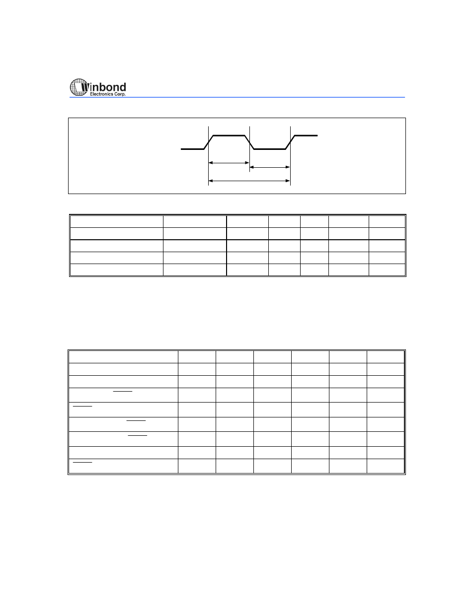
Clock Input Waveform
T
T
XTAL1
F
CH
CL
OP,
T
CP
Continued
PARAMETER
SYMBOL
MIN.
TYP.
MAX.
UNIT
NOTES
Operating Speed
F
OP
0
-
40
MHz
1
Clock Period
T
CP
25
-
-
nS
2
Clock High
T
CH
10
-
-
nS
3
Clock Low
T
CL
10
-
-
nS
3
Notes:
1. The clock may be stopped indefinitely in either state.
2. The T
CP
specification is used as a reference in other specifications.
3. There are no duty cycle requirements on the XTAL1 input.
Program Fetch Cycle
External Program Memory Fetch Cycle (see Figure 6)
PARAMETER
SYMBOL
MIN.
TYP.
MAX.
UINT
NOTES
Address Valid to ALE Low
T
AAS
1T
CP
-
∆
-
-
nS
Address Hold After ALE Low
T
AAH
1T
CP
-
∆
-
-
nS
1
ALE Low to PSEN Low
T
APL
1T
CP
-
∆
1T
CP
1T
CP
+
∆
nS
PSEN Low to Data Valid
T
PDA
-
-
2T
CP
nS
2
Data Hold After PSEN High
T
PDH
0
-
1T
CP
nS
3
Data Float After PSEN High
T
PDZ
0
-
1T
CP
nS
ALE Pulse Width
T
ALW
2T
CP
-
∆
2T
CP
2T
CP
+
∆
nS
4
PSEN Pulse Width
T
PSW
3T
CP
-
∆
3T
CP
3T
CP
+
∆
nS
4
Notes:
1. P00-P07, P20-P27 remain stable through entire memory cycle.
2. Memory access time is 3 Tcp.
3. Data has been latched internally prior to /PSEN going high.
4.
∆ is 20 ns (due to buffer driving delay and wire loading).