5 control loop bode diagrams: tps62065, Figure 11 – Texas Instruments TPS62065 User Manual
Page 11

www.ti.com
TPS62065/67EVM Test Data
6.5
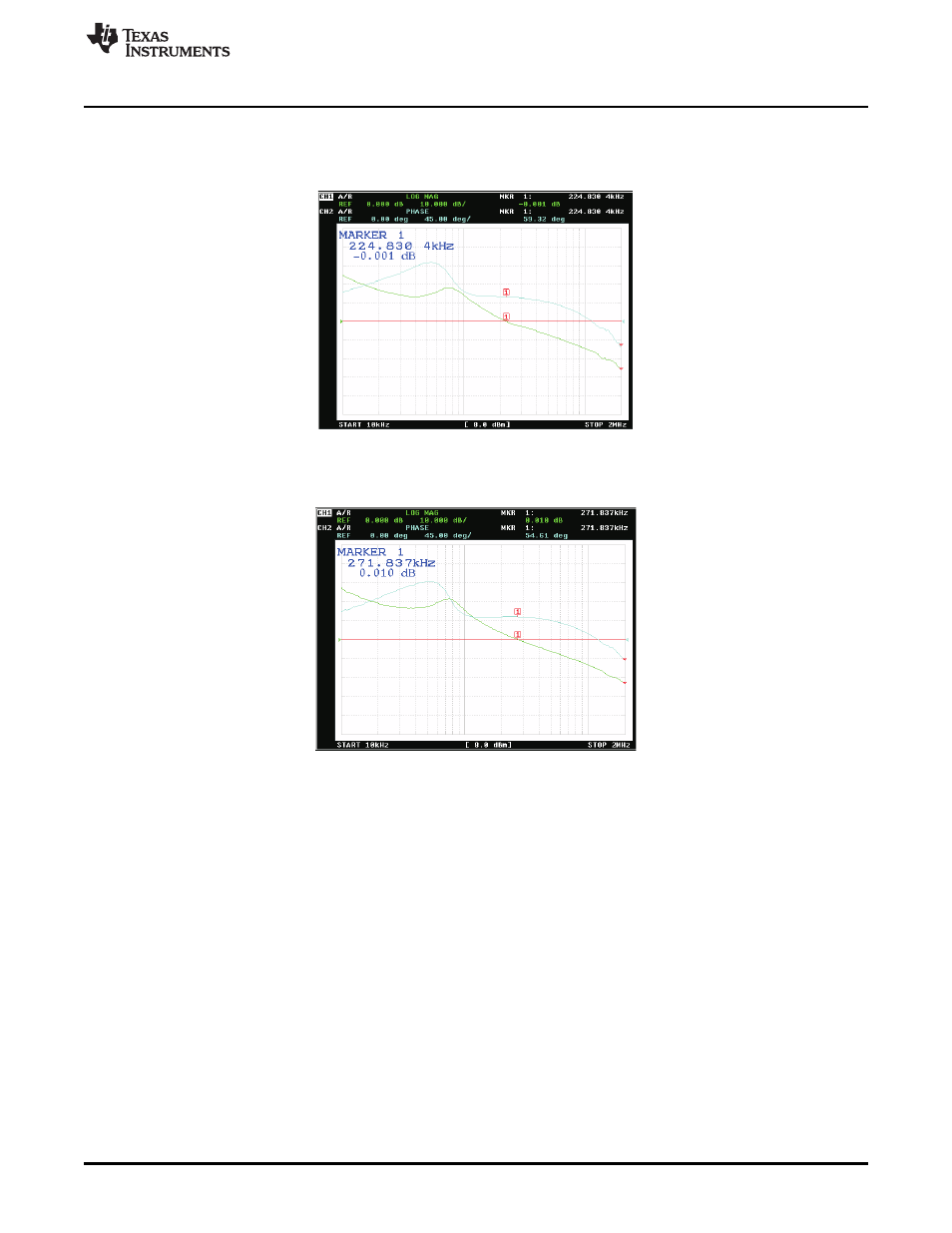
Control Loop Bode Diagrams: TPS62065
and
illustrate typical TPS62065 gain and phase performance versus frequency at VIN
= 3.6 V and 5.0 V, respectively, using the TPS62025EVM.
Conditions: VIN = 3.6 V, VOUT = 1.8 V, I
OUT
= 1.6 A; bandwidth: 224 kHz, phase margin: 59°
Figure 10. TPS62065 Gain and Phase vs Frequency
Conditions: VIN = 5.0 V, VOUT = 1.8 V, I
OUT
= 1.6 A; bandwidth: 271 kHz, phase margin: 54°
Figure 11. TPS62065 Gain and Phase vs Frequency
11
SLVU364 – March 2010
TPS62065/67EVM
Copyright © 2010, Texas Instruments Incorporated
