Texas Instruments TMS320C645X User Manual
Page 10

Overview
General-Purpose Input/Output (GPIO)
10
SPRU724
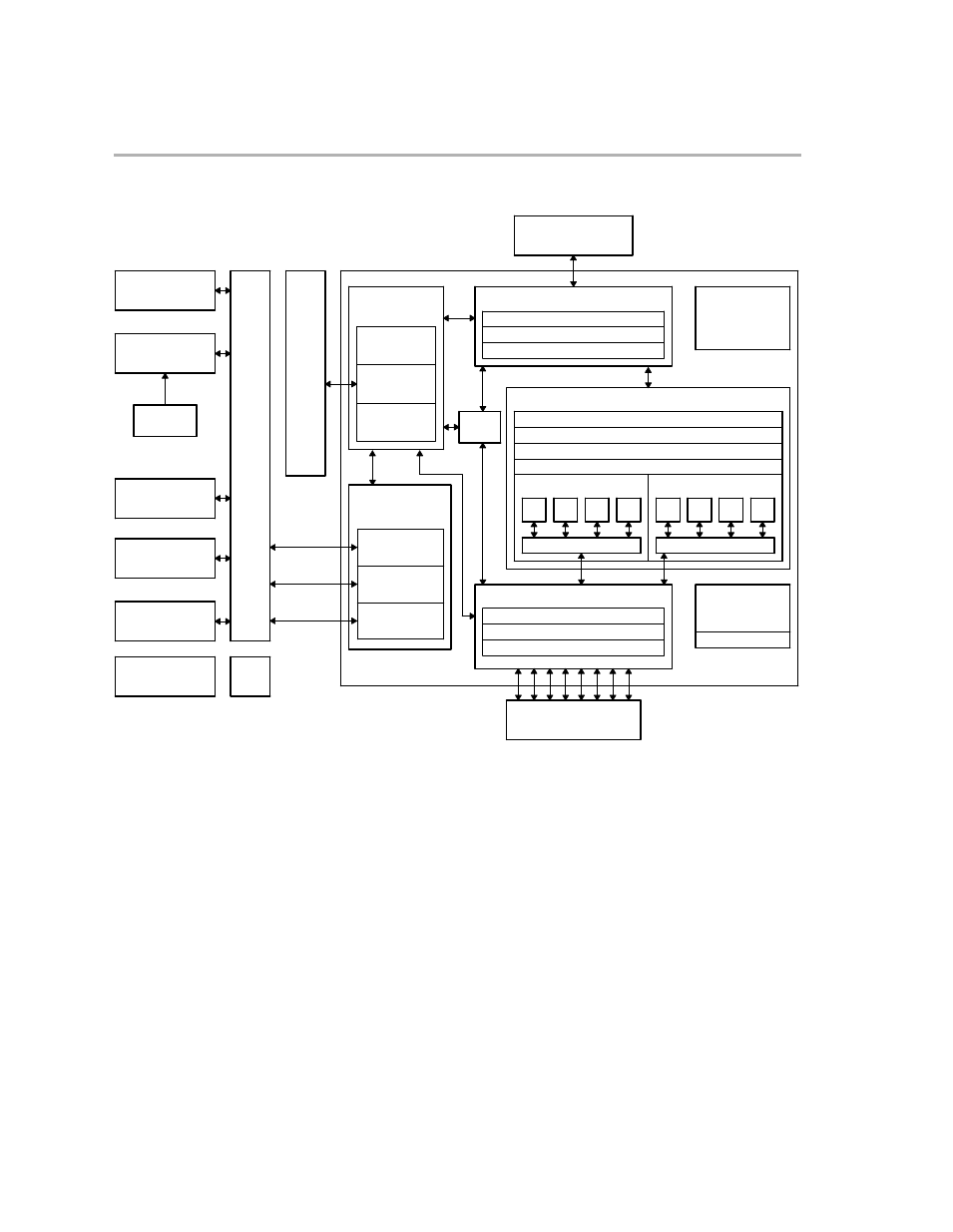
Figure 1.
TMS320C645x DSP Block Diagram
L1
S1
M1
D1
Data path A
Register file A
Register file B
D2
Data path B
S2
M2
L2
L1 data memory controller
Cache control
Memory protection
Interrupt
and exception
controller
Power control
Instruction decode
16/32−bit instruction dispatch
Instruction fetch
SPLOOP buffer
C64x+ CPU
IDMA
Bandwidth management
Cache control
L1 program memory controller
Advanced
event
triggering
(AET)
L2 memory
controller
Bandwidth
management
Memory
protection
registers
Configuration
L1P
cache/SRAM
L1D
cache/SRAM
PLL2
DDR2 memory
EMIFA
Other
peripherals
EDMA
Boot
configuration
Switched central resource
PLL2
L2 memory
controller
controller
memory
External
controller
DMA
Master
DMA
Slave
Cache
control
Bandwidth management
Memory protection
GPIO
Some GPIO pins are MUXed with other device pins. Refer to the device-specific
datasheet for details on specific MUXing and for the availability of the register
bits. GPINT[0:15] are all available as synchronization events to the EDMA
controller and as interrupt sources to the CPU.
