Rev. a – Texas Instruments THS3001 User Manual
Page 9
Description
1-3
General Information
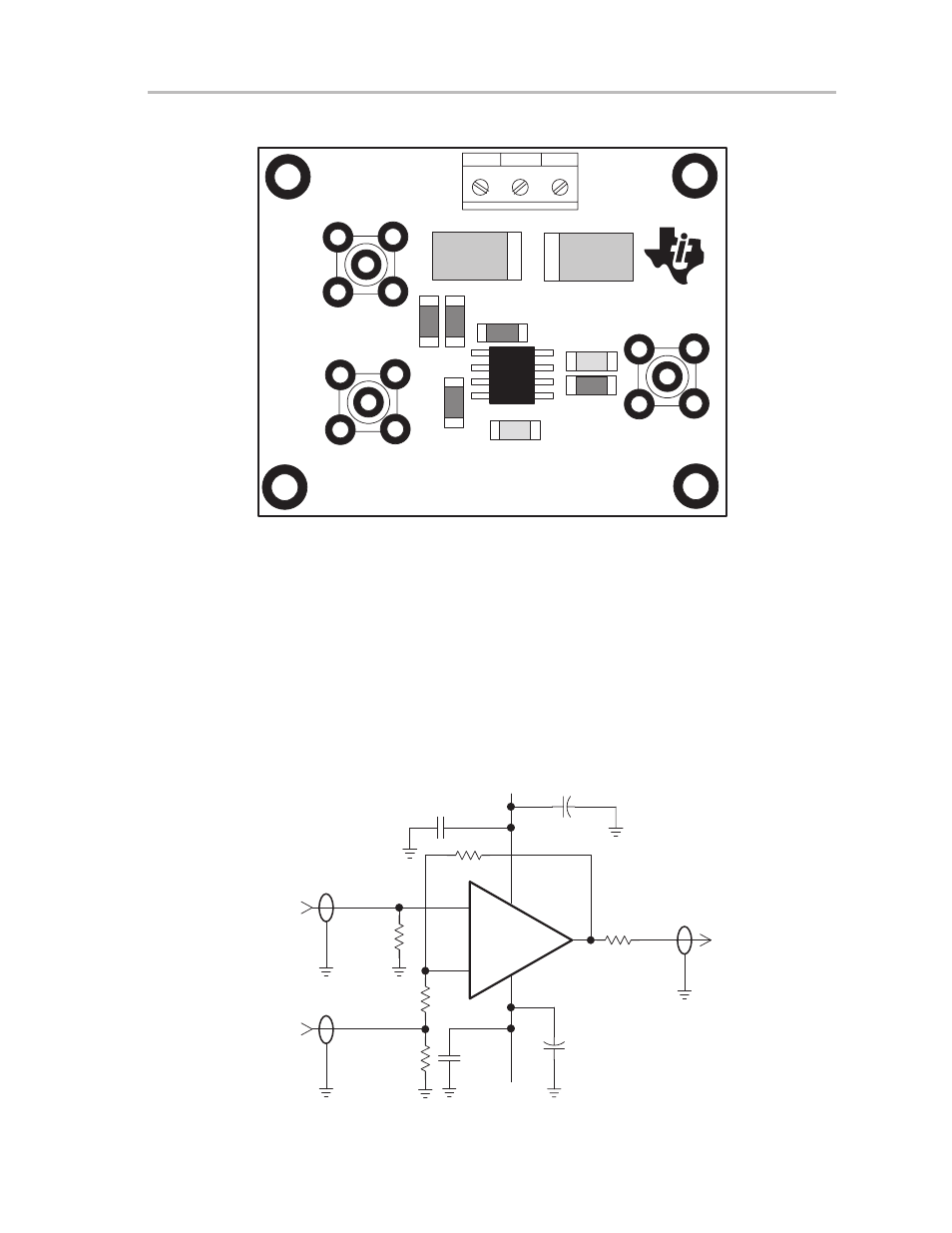
Figure 1–2. THS3001 Rev. A Evaluation Module
NONINVERTING
+
R4
R2
+VCC
C1
R1
C3
C2
GND
–VCC
R5
C4
R3
U1
J2
–IN
GND
J4
OUT
GND
J3
+IN
GND
INVERTING
SLOP130 Rev A
THS3001 EVM Board
J1
INSTRUMENTS
+
TEXAS
Rev. A
The THS3001 EVM is equipped with both noninverting and inverting inputs.
The noninverting input is set for a gain of 2 and the inverting input is set for a
gain of 1. Each input is terminated with a 50-
Ω
resistor to provide correct line
impedance matching (Figure 1–3 for original version and Figure 1–4 for Rev.
A). The amplifier IC output is routed through a 50-
Ω
resistor both to provide
correct line impedance matching and to help isolate capacitive loading on the
output of the amplifier. Capacitive loading directly on the output of the IC
decreases the amplifier’s phase margin and can result in peaking or
oscillations.
Figure 1–3. THS3001 EVM Schematic – Original Version
Non-
Inverting
Input
Inverting
Input
V
CC
Output
R3
49.9
Ω
R1
1 k
Ω
C4
0.1
µ
F
R5
1 k
Ω
R4
49.9
Ω
C3
6.8
µ
F/35 V
–V
CC
2
3
4
6
7
+
–
U1
THS3001
R2
49.9
Ω
J1
J2
+
C2
0.1
µ
F
+
C1
6.8
µ
F/35 V
J3