Transcend Information Secure Digital Card TS2GSD150 User Manual
Page 9
T
T
T
S
S
S
2
2
2
G
G
G
S
S
S
D
D
D
1
1
1
5
5
5
0
0
0
2GB 150x Secure Digital Card
Transcend Information Inc.
9
4. Relative Card Address Register (RCA)
The writable 16-bit relative card address register carries the card address assigned by the host during the card
identification. This address is used for the addressed host-card communication after the card identification procedure.
The default value of the RCA register is 0x0001. The value 0x0000 is reserved to set all cards into the Stand-by State
with CMD7. In SD mode, the value of this register is generated by random number generator inside the card. Please
reference to SD specification for detail information.
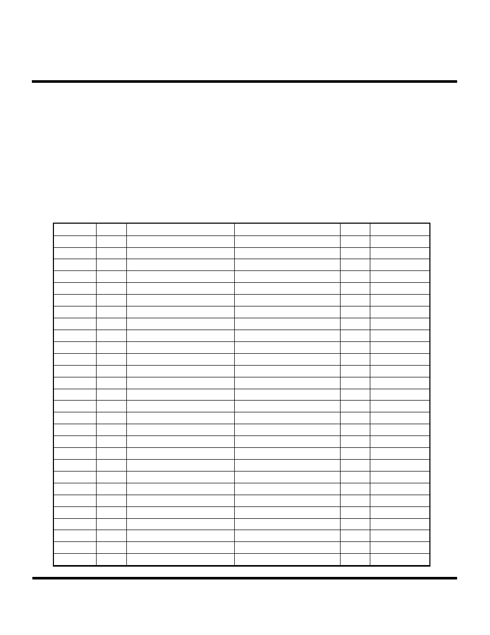
5. Card Specific Data Register (CSD)
The Card-Specific Data register provides information on how to access the card contents. The CSD defines the data
format, error correction type, maximum data access time, data transfer speed, whether the DSR register can be used
etc. The programmable part of the register can be changed by CMD27.
CSD bit
Width
Name
Field
Value
Note
[127:126] 2
CSD
structure
CSD_STRUCTURE 00
b v1.0
[125:120] 6
Reserved
---
---
---
[119:112]
8
Data read access-time 1
TAAC
7F h
80 ms
[111:104]
8
Data read access-time 2
NSAC
FF h
25.5k clocks
[103:96]
8
Max. bus clock freq.
TRAN_SPEED
32 h
25 MHz
[95:84]
12
Card command classes
CCC
1F5 h
(*1)
[83:80]
4
Max. read data block length
READ_BL_LEN
9 h
512 bytes
[79]
1
Partial block read allowed
READ_BL_PARTIAL
1 b
Support
[78]
1
Write block misalignment
WRITE_BLK_MISALIGN
1 b
Support
[77]
1
Read block misalignment
READ_BLK_MISALIGN 1
b Support
[76]
1
DSR implemented
DSR_IMP
0 b
Not support
[75:74] 2
Reserved
---
---
---
[73:62] 12
Device
size
C_SIZE
(*2)
(*2)
[61:59]
3
Max. R_curr @
VDD
min
VDD_R_CURR_MIN
101 b
35 mA
[58:56]
3
Max R_curr @
VDD
max
VDD_R_CURR_MAX
101 b
45 mA
[55:53]
3
Max W_curr @
VDD
min
VDD_W_CURR_MIN
101 b
35 mA
[52:50]
3
Max W_curr @
VDD
max
VDD_W_CURR_MAX
101 b
45 mA
[49:47]
3
Device size multiplier
C_SIZE_MULT
(*2)
(*2)
[46]
1
Erase single block enable
ERASE_BLK_EN
0 b
Not allowed
[45:39]
7
Erase sector size
SECTOR_SIZE
(*3)
(*3)
[38:32]
7
Write protect group size
WP_GRP_SIZE
(*4)
(*4)
[31]
1
Write protect group enable
WP_GRP_ENABLE
1 b
Support
[30:29] 2
Reserved
---
---
---
[28:26]
3
Write speed factor
R2W_FACTOR
101 b
32X
[25:22]
4
Max. write data block length
WRITE_BL_LEN
9 h
512 bytes
[21]
1
Partial block write allowed
WRITE_BL_PARTIAL
1 b
Support
[20:16] 5
Reserved
---
---
---
[15]
1
File format group
FILE_FORMAT_GRP
0 b
HD like FAT