Electrical characteristics – Oki MSM66P201 User Manual
Page 19

19/30
¡ Semiconductor
MSM66201/66P201/66207/66P207
ELECTRICAL CHARACTERISTICS
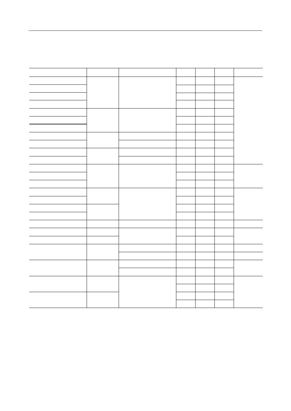
DC Characteristics
Note: 1 Applied to P0
2 Applied to P1, P2, P3 and P4
3 Applied to P5
4 Applied to ALE, PSEN, RD, WR and RESOUT
5 Applied to RES and NMI
6 Applied to READY and EA
7 Applied to FLT
8 Applied to OSC
0
*
V
DD
or GND for ports serving as the input pin. No load for any other.
** Applied to MSM66P201/66P207
Parameter
Symbol
Condition
Min.
Max.
Unit
"H" Input Voltage 1, 3, 6
"H" Input Voltage 5, 7
V
IH
2.4
4.0
4.2
3.6
V
DD
+0.3
V
DD
+0.3
V
DD
+0.3
V
DD
+0.3
—
"H" Input Voltage 8
"H" Input Voltage 2
Typ.
—
"L" Input Voltage 1, 2, 3, 6
V
IL
–0.3
–0.3
–0.3
0.8
0.8
0.4
V
"L" Input Voltage 5, 7
"L" Input Voltage 8
V
OH
4.2
4.2
—
—
I
O
= –400mA
"H" Output Voltage 1, 4
"H" Output Voltage 2
V
OL
—
—
0.4
0.4
I
O
= 3.2mA
"L" Output Voltage 1, 4
"L" Output Voltage 2
I
O
= –200mA
I
O
= 1.6mA
Input Leakage Current 3, 6, 7
I
IH
/I
IL
—
—
—
1/–1
1/–20
10/–10
mA
V
I
= V
DD
/0V
Input Current 5
Input Current 8
"H" Output Current 1
"H" Output Current 2
I
OH
I
OL
–2
–1
10
5
—
—
—
—
mA
V
O
= 2.4V
"L" Output Current 1
"L" Output Current 2
I
LO
—
±2
mA
Output Leakage Current 1, 2, 4
V
O
= V
DD
/0V
C
I
C
O
—
—
—
—
pF
Input Capacitance
Output Capacitance
5
7
f = 1MHz
Ta = 25°C
I
DDS
—
—
10
100
mA
Current Consumption
(during STOP) *
0.2
1
V
DD
= 2V
I
DDH
—
**
—
10
15
Current Consumption
(during HALT)
6
8
f
OSC
= 10MHz
No Load
I
DD
—
**
—
35
40
mA
Current Consumption
20
30
—
—
—
—
—
—
—
—
—
—
—
—
—
—
—
—
—
—
—
(V
DD
= 5V ± 10%, Ta = –40 to +85°C)
I
REF
—
—
2
10
Analog Reference Power
Supply Current
0.3
0.5
A/D in operation
A/D stopped
mA
mA
—
