Table 6. ni 656x ddc connector pins, Ble 6 – National Instruments PXI-6561/6562 User Manual
Page 24
NI Digital Waveform Generator/Analyzer Guide
24
ni.com
Note
If you are designing a custom cabling solution with
connector (779157-01) and cable (192744-01), the NI665X pinout
is reversed at the end connector. For example, the signal shown on
pin 1 shown in the previous figure would map to pin 73 at the end
connector.
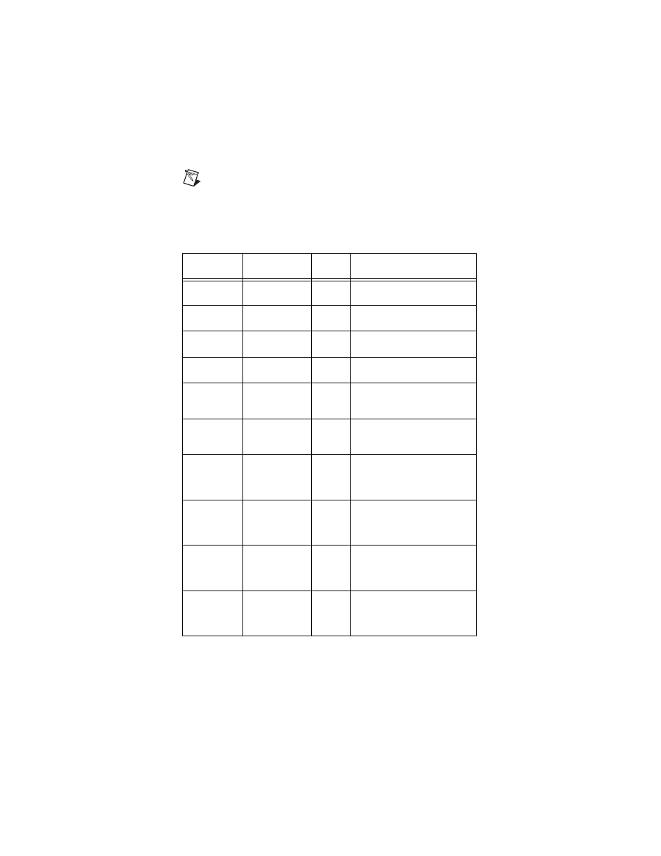
Table 6. NI 656X DDC Connector Pins
Pins
Signal Name
Signal
Type
Signal Description
65
DDC CLK OUT
LVDS
Control
Positive terminal for the exported
Sample clock.
66
DDC CLK OUT
LVDS*
Control
Complementary terminal for the
LVDS exported Sample clock.
71
DDC CLK OUT
LVPECL
Control
Positive terminal for the LVPECL
exported Sample clock.
72
DDC CLK OUT
LVPECL*
Control
Complementary terminal for the
LVPECL exported Sample clock.
62
STROBE
Control
Positive external Sample clock
source which can be used for
dynamic acquisition.
63
STROBE*
Control
Complementary external Sample
clock source which can be used for
dynamic acquisition.
14, 17, 20, 23,
26, 29, 32, 35,
38, 41, 44, 47,
50, 53, 56, 59
DIO <0..15>
Data
Bidirectional digital I/O data
channels 0 through 15.
15, 18, 21, 24,
27, 30, 33, 36,
39, 42, 45, 48,
51, 54, 57, 60
DIO <0..15>*
Data
Complementary bidirectional
digital I/O data channels
0 through 15.
2, 5, 8
PFI<1..3>
Control
Positive input terminals to the
NI 656X for external triggers, or
output terminals from the NI 656X
for events.
3, 6, 9
PFI<1..3>*
Control
Complementary input terminals to
the NI 656X for external triggers,
or output terminals for the
NI 656X for events.