E select (see, Figure 42, Nxp semiconductors – NXP Semiconductors P89LPC9321 UM10310 User Manual
Page 91
UM10310
All information provided in this document is subject to legal disclaimers.
© NXP B.V. 2010. All rights reserved.
User manual
Rev. 2 — 1 November 2010
91 of 139
NXP Semiconductors
UM10310
P89LPC9321 User manual
(1) Not defined
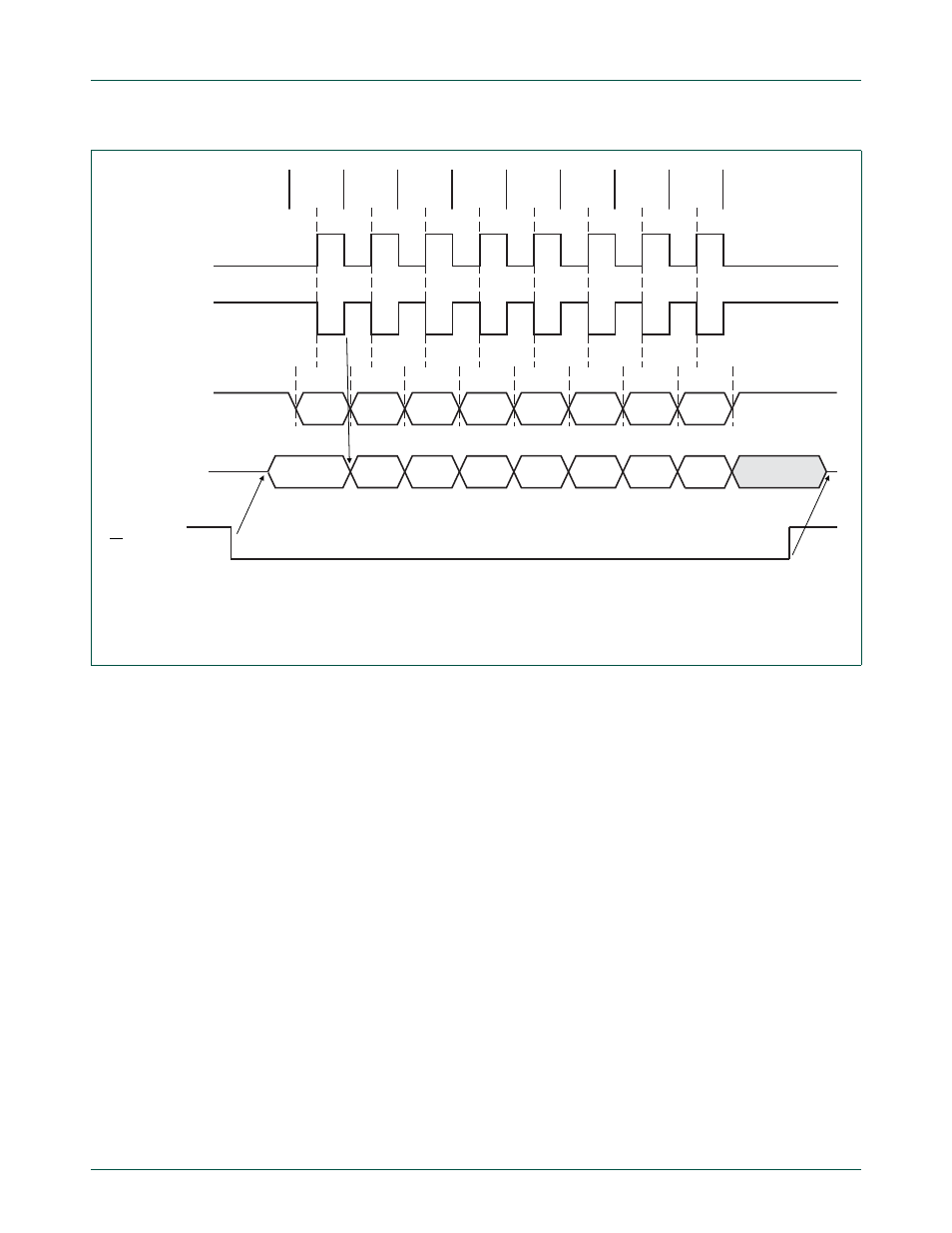
Fig 42. SPI slave transfer format with CPHA = 0.
1
2
3
4
5
6
7
8
MSB
LSB
DORD = 0
DORD = 1
6
1
5
2
4
3
3
4
2
5
1
6
LSB
MSB
MSB
LSB
DORD = 0
DORD = 1
6
1
5
2
4
3
3
4
2
5
1
6
LSB
MSB
(1)
002aaa934
Clock cycle
SPICLK (CPOL = 0)
SPICLK (CPOL = 1)
MOSI (input)
MISO (output)
SS (if SSIG bit = 0)