1 configuring the spi, Figure 41, Table 82 – NXP Semiconductors P89LPC9321 UM10310 User Manual
Page 88: Nxp semiconductors
UM10310
All information provided in this document is subject to legal disclaimers.
© NXP B.V. 2010. All rights reserved.
User manual
Rev. 2 — 1 November 2010
88 of 139
NXP Semiconductors
UM10310
P89LPC9321 User manual
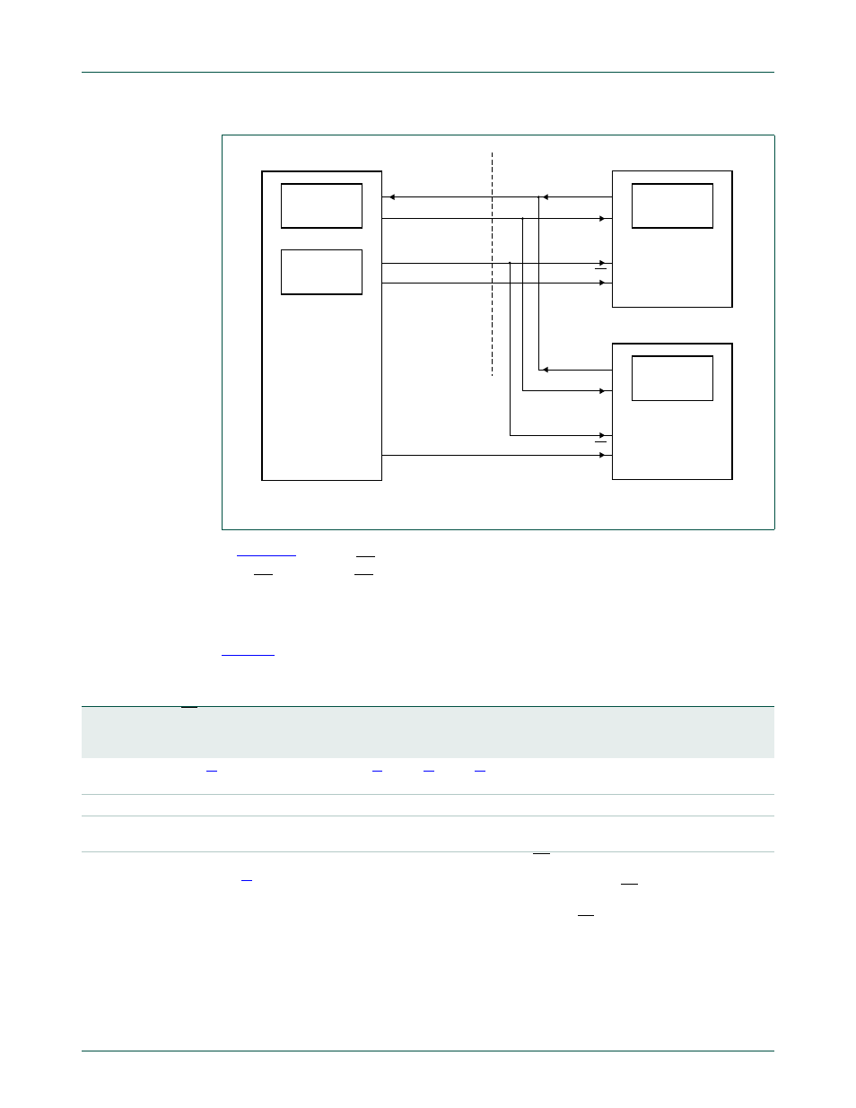
, SSIG (SPCTL.7) bits for the slaves are logic 0, and the slaves are selected
by the corresponding SS signals. The SPI master can use any port pin (including
P2.4/SS) to drive the SS pins.
12.1 Configuring
the
SPI
shows configuration for the master/slave modes as well as usages and
directions for the modes.
Fig 41. SPI single master multiple slaves configuration.
002aaa903
master
slave
8-BIT SHIFT
REGISTER
SPI CLOCK
GENERATOR
8-BIT SHIFT
REGISTER
MISO
MOSI
SPICLK
port
port
MISO
MOSI
SPICLK
SS
slave
8-BIT SHIFT
REGISTER
MISO
MOSI
SPICLK
SS
Table 82.
SPI master and slave selection
SPEN
SSIG
SS Pin MSTR
Master
or Slave
Mode
MISO
MOSI
SPICLK Remarks
0
x
P2.4
x
SPI
Disabled
P2.3
SPI disabled. P2.2, P2.3, P2.4, P2.5 are used
as port pins.
1
0
0
0
Slave
output
input
input
Selected as slave.
1
0
1
0
Slave
Hi-Z
input
input
Not selected. MISO is high-impedance to avoid
bus contention.
1
0
0
1 (->
0)
Slave
output
input
input
P2.4/SS is configured as an input or
quasi-bidirectional pin. SSIG is 0. Selected
externally as slave if SS is selected and is
driven low. The MSTR bit will be cleared to
logic 0 when SS becomes low.