Absolute maximum ratings, Dc electrical characteristics, Μa747c dual operational amplifier – NXP Semiconductors UA747C User Manual
Page 2

Philips Semiconductors Linear Products
Product specification
µ
A747C
Dual operational amplifier
August 31, 1994
55
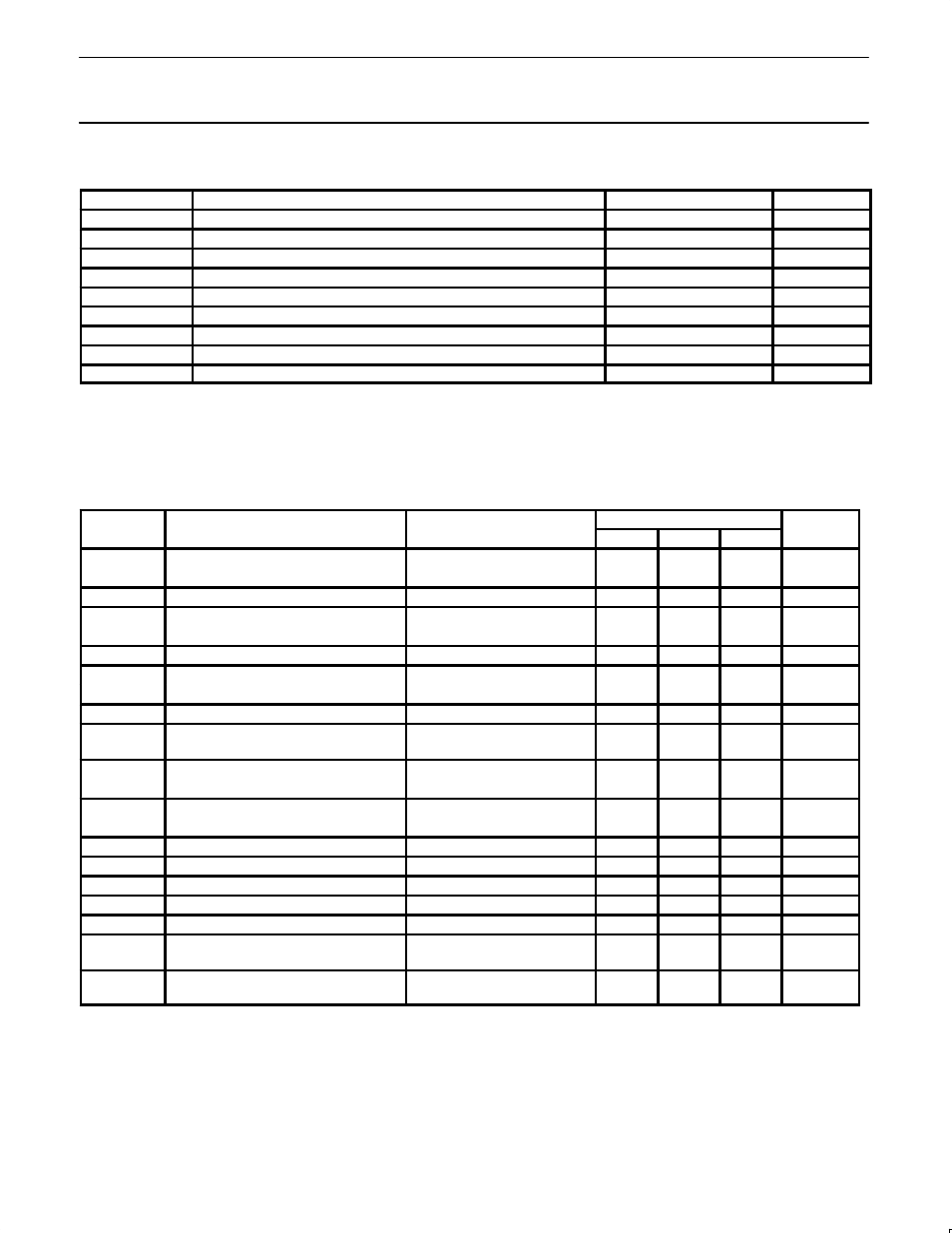
ABSOLUTE MAXIMUM RATINGS
SYMBOL
PARAMETER
RATING
UNIT
V
S
Supply voltage
±
18
V
P
D MAX
Maximum power dissipation T
A
=25
°
C (still air)
1
1500
mW
V
IN
Differential input voltage
±
30
V
V
IN
Input voltage
2
±
15
V
Voltage between offset null and V-
±
0.5
V
T
STG
Storage temperature range
-65 to +150
°
C
T
A
Operating temperature range
0 to +70
°
C
T
SOLD
Lead temperature (soldering, 10sec)
300
°
C
I
SC
Output short-circuit duration
Indefinite
NOTES:
1. Derate above 25
°
C at the following rates:
N package at 12mW/
°
C
2. For supply voltages less than
±
15V, the absolute maximum input voltage is equal to the supply voltage.
DC ELECTRICAL CHARACTERISTICS
T
A
=25
°
C, V
CC
=
±
15V unless otherwise specified.
SYMBOL
PARAMETER
TEST CONDITIONS
µ
A747C
UNIT
SYMBOL
PARAMETER
TEST CONDITIONS
Min
Typ
Max
UNIT
V
OS
Offset voltage
R
S
≤
10k
Ω
2.0
6.0
mV
R
S
≤
10k
Ω
, over temp.
3.0
7.5
mV
∆
V
OS
/
∆
T
10
µ
V/
°
C
I
OS
Offset current
20
200
nA
Over temperature
7.0
300
nA
∆
I
OS
/
∆
T
200
pA/
°
C
I
BIAS
Input current
80
500
nA
Over temperature
30
800
nA
∆
I
B
/
∆
T
1
nA/
°
C
V
OUT
Output voltage swing
R
L
≥
2k
Ω
, over temp.
R
L
≥
10k
Ω
, over temp.
±
10
±
12
±
13
±
14
V
V
I
CC
Supply current each side
1.7
2.8
mA
Over temperature
2.0
3.3
mA
P
d
Power consumption
50
85
mW
Over temperature
60
100
mW
C
IN
Input capacitance
1.4
pF
Offset voltage adjustment range
±
15
mV
R
OUT
Output resistance
75
Ω
Channel separation
120
dB
PSRR
Supply voltage rejection ratio
R
S
≤
10k
Ω
, over temp.
30
150
µ
V/V
A
VOL
Large-signal voltage gain (DC)
R
L
≥
2k
Ω
, V
OUT
=
±
10V
Over temperature
25,000
15,000
V/V
V/V
CMRR
Common-mode rejection ratio
R
S
≤
10k
Ω
, V
CM
=
±
12V
Over temperature
70
dB
