Pinning information, 1 pinning, 2 pin description – Philips TDA9964 User Manual
Page 4: Tda9964, Philips semiconductors, 1 pinning 7.2 pin description
Philips Semiconductors
TDA9964
12-bit, 3.0 V, 30 Msps analog-to-digital interface for CCD cameras
Objective specification
Rev. 03 — 16 January 2001
4 of 23
9397 750 07918
© Philips Electronics N.V. 2001. All rights reserved.
7.
Pinning information
7.1 Pinning
7.2 Pin description
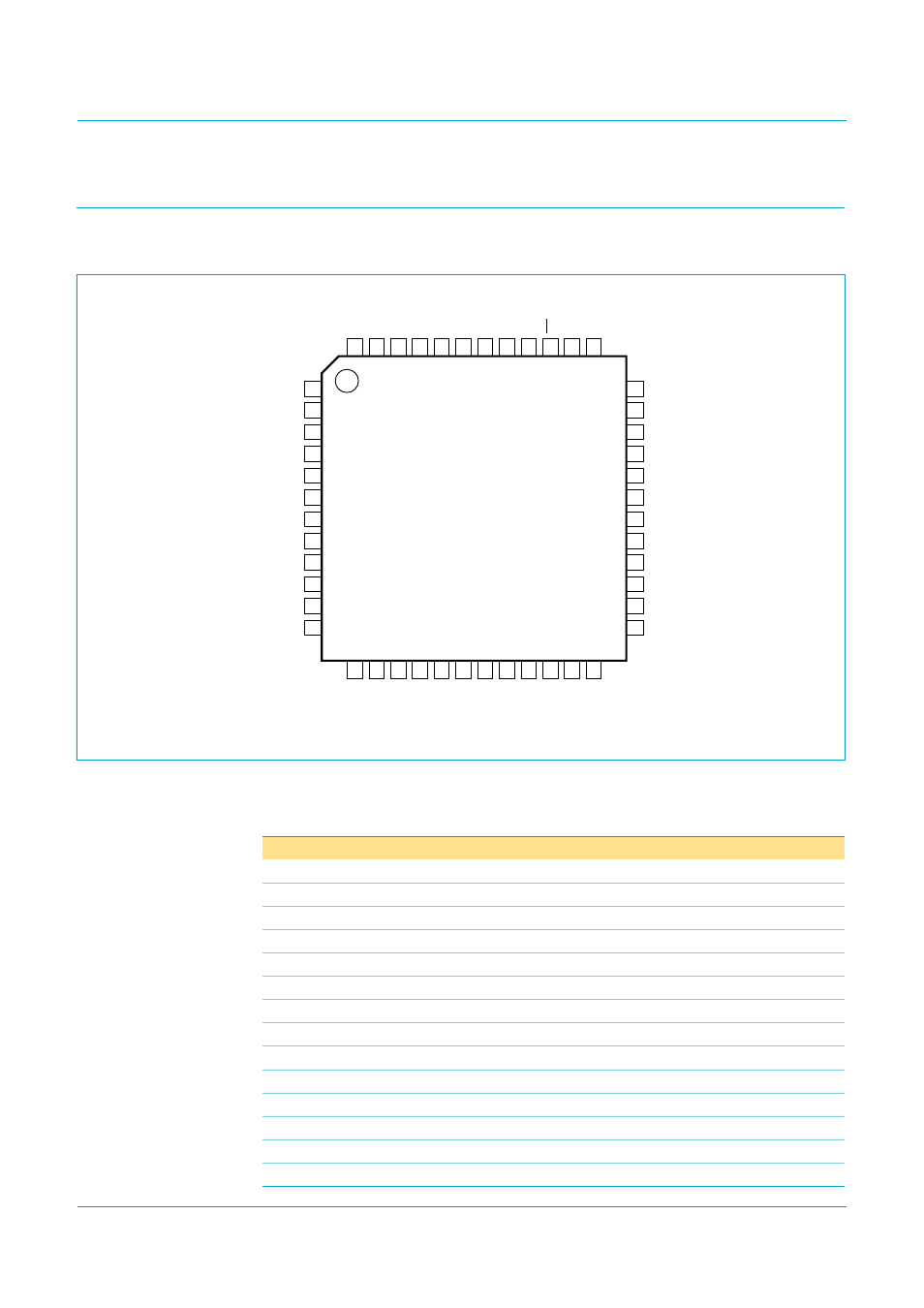
Fig 2.
Pin configuration.
1
2
3
4
5
6
7
8
9
10
11
36
35
34
33
32
31
30
29
28
27
26
13
14
15
16
17
18
19
20
21
22
23
48
47
46
45
44
43
42
41
40
39
38
12
24
37
25
TDA9964HL
FCE516
D9
D10
D11
D8
D7
D6
D4
D3
D2
D1
D0
VCCA1
AGND1
AGND2
IN
AGND3
AGND4
VCCA2
CPCDS1
CPCDS2
OFDOUT
TEST
D5
CLK
SHD
SHP
CLPOB
BLK
STDBY
A
GND6
OGND2
OE
V
CCO2
CLPDM
V
CCA4
DCLPC
OPGA
C
OPGA
A
GND5
V
CCA3
V
CCD1
V
CCO1
DGND1
SCLK
SEN
OGND1
VSYNC
S
D
ATA
Table 3:
Pin description
Symbol
Pin
Description
V
CCA1
1
analog supply voltage 1
AGND1
2
analog ground 1
AGND2
3
analog ground 2
IN
4
input signal from CCD
AGND3
5
analog ground 3
AGND4
6
analog ground 4
V
CCA2
7
analog supply voltage 2
CPCDS1
8
clamp storage capacitor pin 1
CPCDS2
9
clamp storage capacitor pin 2
DCLPC
10
regulator decoupling pin
OFDOUT
11
analog output of the additional 8-bit control DAC
TEST
12
test mode input pin (should be connected to AGND5)
AGND5
13
analog ground 5
V
CCA3
14
analog supply 3